Chapter 2. Architecture and technical overview 45
2.1.4 Memory access
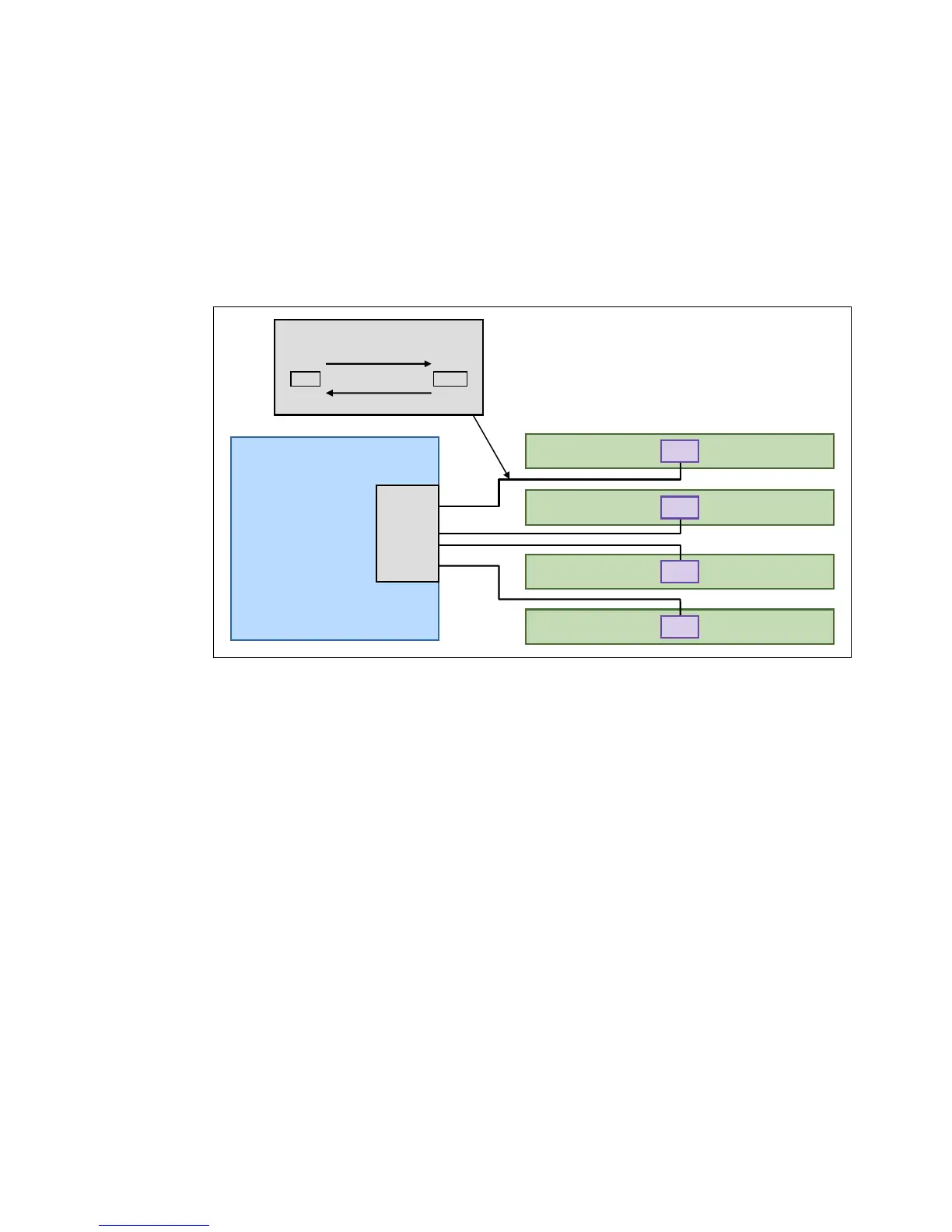
Each POWER7+ processor chip has one DDR3 memory controller, which uses four memory
channels to connect to its quad of DIMMs. Each channel operates at 1066 MHz and can
address up to 64 GB of memory. Thus, each POWER7+ processor chip is capable of
addressing up to 256 GB of memory. The whole system can address up to 4TB of total
memory.
Figure 2-4 gives a simple overview of the POWER7+ processor memory access structure.
Figure 2-4 Overview of POWER7+ memory access structure
2.1.5 On-chip L3 cache innovation and Intelligent Cache
A breakthrough in material engineering and microprocessor fabrication enabled IBM to
implement the L3 cache in eDRAM and place it on the POWER7+ processor die. L3 cache is
critical to a balanced design, as is the ability to provide good signaling between the L3 cache
and other elements of the hierarchy, such as the L2 cache or SMP interconnect.
The on-chip L3 cache is organized into separate areas with differing latency characteristics.
Each processor core is associated with a Fast Local Region of L3 cache (FLR-L3) but also
has access to other L3 cache regions as shared L3 cache. Additionally, each core can
negotiate to use the FLR-L3 cache associated with another core, depending on reference
patterns. Data can also be cloned to be stored in more than one core’s FLR-L3 cache, again
depending on reference patterns. This
Intelligent Cache management enables the POWER7+
processor to optimize the access to L3 cache lines and minimize overall cache latencies.
Memory Channel Description
P7+
SCM
DIMMCPU
Downstream Link
13 + 2 + 1
Upstream Link
20 + 2 + 1
SN DIMM 1
SN DIMM 2
SN DIMM 3
SN DIMM 4
MEM
Cntl 0
A
B
C
D
SN
SN
SN
SN