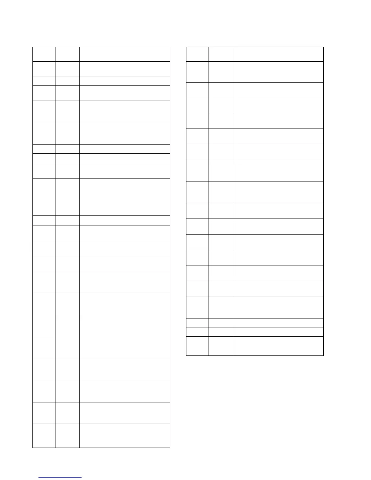
Pin Port
Description
number name
Pin Port
Description
number name
4 - 4
4-6 PORT ALLOCATIONS
4-6-1 CPU (IC8)
1
9
11
12
14
16
17
19
21
23–25
26
28–30
32–35
44–47
48
49
50
51
52
53
54
55
DICK
RESET
CSIFT
SCK
SO
CLIN
CLOUT
NOIS
S1
OPV1–
OPV3
CONT
V3–V1
COM4–
COM1
KR3–
KR0
UNLK
RMUT
MMUT
DUSE
PCON
R5C
T5C
TXC
Input port for the clock signal from the
[DIAL] (S801).
Input port for reset signal.
Outputs reference oscillator for the
CPU control signal.
Outputs serial clock signal to the PLL
IC (IC1, pin 2), D/A convertor IC (IC10,
pin 7) and optional unit.
Outputs serial signals to the PLL IC
(IC1, pin 3), D/A convertor IC (IC10,
pin 8) and optional unit.
Input port for the cloning signal.
Outputs the cloning signal.
Input port for noise signals (pulse
type).
Input port for the power switch.
Low : While POWER switch is
pushed.
I/O ports for optional unit detection
signals from/to J5.
Outputs LCD contrast control signal.
Input port for the bias signals for the
LCD.
Outputs LCD common signals.
Input port for initial matrix.
Low : While keys are pushing.
Input port for PLL unlock signal from
the PLL IC (IC1, pin 14).
Low : During lock.
• Outputs RX mute control signal.
• Input port for the RX mute signal
from the optional unit.
• Outputs TX mute control signal.
• Input port for the TX mute signal
from the optional unit.
Outputs low-pass filter cut-off frequen-
cy control signal when DTCS is acti-
vated.
Outputs SW5 regulator (Q55, Q57,
Q39) control signal.
Low : While power is ON.
Outputs R5 regulator (Q21) control
signal.
Low : While receiving.
Outputs T5 regulator (Q22) control
signal.
Low : While transmitting.
Outputs APC circuit (Q37, IC3) control
signal.
High : While transmitting.
56
57
58
59
60
61
62
63
64–87
90
91
94
95
96
97
98
99
100
Outputs control signal for the regulator
circuit of AF power amplifier.
High : When squelch is open, etc.
Outputs LCD backlight control signal.
High : Lights ON.
Outputs EEPROM (IC7, pin 6) clock
signal.
I/O port for the data signals from/to the
EEPROM (IC7, pin 5).
I/O port for strobe signals from/to the
D/A convertor IC (IC10, pin 6).
Outputs strobe signals to the PLL IC
(IC1, pin 4).
Outputs VCO5 regulator (Q11) control
signal.
Low : While power is ON.
Outputs PS5 regulator (Q54) control
signal.
Low : While power is ON.
Output LCD driver signals.
Outputs CTCSS and DTCS tone sig-
nal.
Outputs DTMF, BEEP and 1750 Hz
tone signal.
Input port for CTCSS and DTCS
decoded signals.
Input port for the [PTT] switch.
High : While [PTT] switch is pushed.
Input port for the UP/DOWN signal
from the [DIAL] (S801).
Input port for the remote signals from
an optional microphone (HM-75A) via
the [MIC] jack.
Input port for the RSSI detection.
Input port for the PLL lock voltage.
Input port for the transceiver’s internal
tempareture detection.
AFON
LIGT
ESCK
ESDA
DAST
PLST
PSVCO
PS5C
SEG1–
SEG23
CTCC
TONE
CTCIN
PTT
DIUD
REMO
SD
LVIN
TEMP
 Loading...