TERMINAL DESCRIPTION
IC BLOCK DIAGRAMS AND TERMINAL DESCRIPTIONS -28
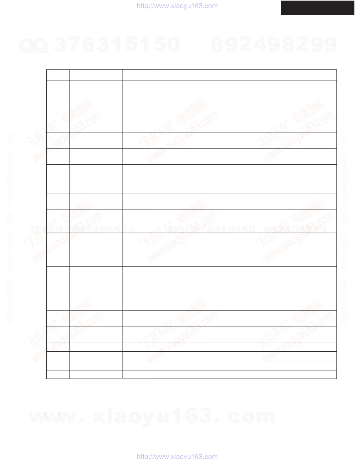
Q3461, Q3561 : IS42S32200E-6TL (64 Mbit SD RAM)
TX-SR806/SA806
Symbol Pin No. Type Function
A0-A10
25 to 27 Input Pin
Address Inputs: A0-A10 are sampled during the ACTIVE
60 to 66
command (row-address A0-A10) and READ/WRITE command (A0-A7
24
with A10 defining auto precharge) to select one location out of the memory array
in the respective bank. A10 is sampled during a PRECHARGE command to
determine if all banks are to be precharged (A10 HIGH) or bank selected by
BA0, BA1 (LOW). The address inputs also provide the op-code during a LOAD
MODE REGISTER command.
BA0, BA1 22,23 Input Pin
Bank Select Address: BA0 and BA1 defines which bank the ACTIVE, READ,
WRITE or PRECHARGE command is being applied.
CAS
18 Input Pin
CAS, in conjunction with the RAS and WE, forms the device command. See the
"Command Truth Table" for details on device commands.
CKE
67 Input Pin
The CKE input determines whether the CLK input is enabled. The next rising edge
of the CLK signal will be valid when is CKE HIGH and invalid when LOW. When
CKE is LOW, the device will be in either power-down mode, clock suspend mode,
or self refresh mode.
CKE is an asynchronous i
nput.
CLK
68 Input Pin
CLK is the master clock input for this device. Except for CKE, all inputs to this
device are acquired in synchronization with the rising edge of this pin.
CS
20 Input Pin
The CS input determines whether command input is enabled within the device.
Command input is enabled when CS is LOW, and disabled with CS is HIGH. The
device remains in the previous state when CS is HIGH.
DQ0 to
2, 4, 5, 7, 8, 10,11,13 DQ Pin
DQ0 to DQ15 are DQ pins. DQ through these pins can be controlled in byte units
DQ31
74,76,77,79,80,82,83,85
using the DQM0-DQM3 pins
45,47,48,50,51,53,54,56
31,33,34,36,37,39,40,42
DQM0
16,28,59,71 Input Pin
DQMx control thel ower and upper bytes of the DQ buffers. In read mode,
DQM3
the output buffers are place in a High-Z state. During a WRITE cycle the input data is
masked. When DQMx is sampled HIGH and is an input mask signal for write accesses
and an output enable signal for read accesses. DQ0 through DQ7 are controlled by
DQM0. DQ8 throughDQ15 are controlled by DQM1. DQ16 through DQ23 are
controlled by DQM2. DQ24 through DQ31 are controlled by DQM3.
RAS
19 Input Pin
RAS, in conjunction with CAS and WE, forms the device command. See the "Command
Truth Table" item for details on device commands.
WE
17 Input Pin
WE, in conjunction with RAS and CAS, forms the device command. See the "Command
Truth Table" item for details on device commands.
VDDQ
3,9,35,41,49,55,75,81 Supply Pin
VDDQ is the output buffer power supply.
VDD
1,15,29,43 Supply Pin
VDD is the device internal power supply.
GNDQ
6,12,32,38,46,52,78,84 Supply Pin
GNDQ is the output buffer ground.
GND
44,58,72,86 Supply Pin
GND is the device internal ground.
w
w
w
.
x
i
a
o
y
u
1
6
3
.
c
o
m
Q
Q
3
7
6
3
1
5
1
5
0
9
9
2
8
9
4
2
9
8
T
E
L
1
3
9
4
2
2
9
6
5
1
3
9
9
2
8
9
4
2
9
8
0
5
1
5
1
3
6
7
3
Q
Q
TEL 13942296513 QQ 376315150 892498299
TEL 13942296513 QQ 376315150 892498299
http://www.xiaoyu163.com
http://www.xiaoyu163.com
 Loading...