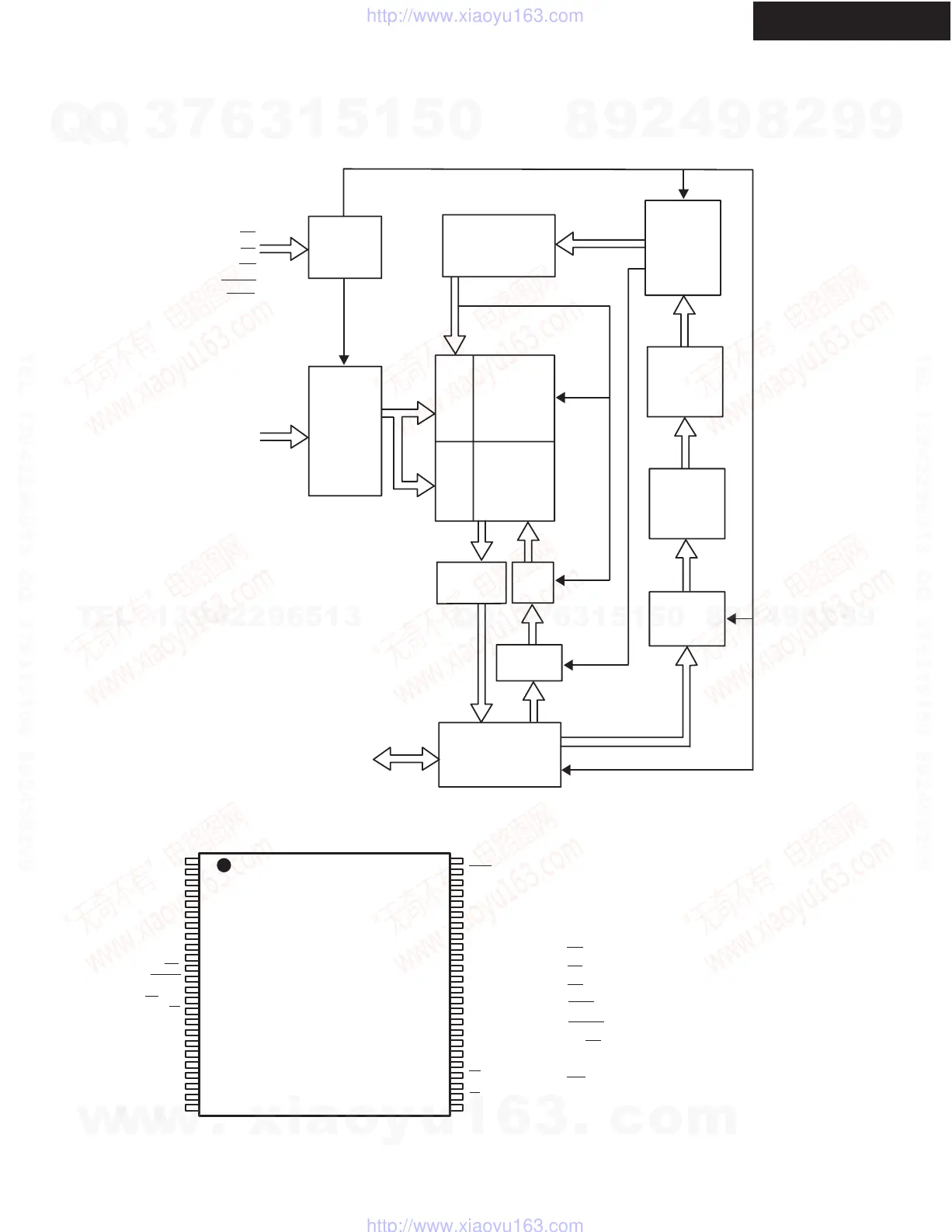
CONTROL
INPUT
LOGIC
PROGRAM/ERASE
HIGH VOLTAGE
WRITE
STATE
MACHINE
(WSM)
REGISTER
STATE
MX29LV320AT/B
FLASH
ARRAY
X-DECODER
Y-DECODER
ADDRESS
LATCH
AND
BUFFER
Y-PASS GATE
PGM
DATA
HV
COMMAND
DATA
DECODER
COMMAND
DATA LATCH
PROGRAM
DATA LATCH
I/O BUFFER
SENSE
AMPLIFIER
Q0-Q15/A-1
A0~A20
WE
OE
WP
RESET
BYTE
BLOCK DIAGRAM
PIN DESCRIPTION
PIN NAME
DESCRIPTION
A0~A20 Address Input
Q0~Q14 Data Input/Output
CE Chip Enable Input
WE Write Enable Input
RESET Hardware Reset Pin/Sector Protect Unlock
OE Output Enable Input
VCC Power Supply Pin (+5V)
GND Ground Pin
Q8005 MX29LV320(32Mbit CMOS Flash memory)
Q15/A-1
BYTE
RY/BY
WP/ACC Hardware Write Protect/Acceleration Pin
Q15:Data Input/Output,word mode
A-1:LSB Address Input,byte mode
Word/Byte Selection Pin
Read/Busy output
MX29LV320AT/B
1
2
3
4
5
6
7
8
9
10
11
12
13
14
15
16
17
18
19
20
21
22
23
24
48
47
46
45
44
43
42
41
40
39
38
37
36
35
34
33
32
31
30
29
28
27
26
25
A15
A14
A13
A12
A11
A10
A9
A8
A19
A20
WE
RESET
NC
WP/ACC
RY/BY
A18
A17
A7
A6
A5
A4
A3
A2
A1
A16
BYTE
GND
Q15/A-1
Q7
Q14
Q6
Q13
Q5
Q12
Q4
VCC
Q11
Q3
Q10
Q2
Q9
Q1
Q8
Q0
OE
GND
CE
A0
IC BLOCK DIAGRAMS AND TERMINAL DESCRIPTIONS -53
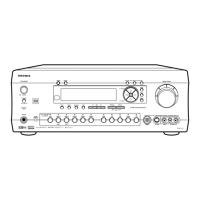
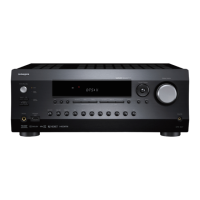
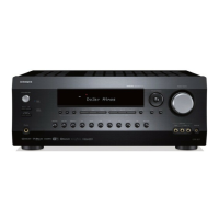
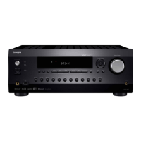
TX-SR806/SA806
w
w
w
.
x
i
a
o
y
u
1
6
3
.
c
o
m
Q
Q
3
7
6
3
1
5
1
5
0
9
9
2
8
9
4
2
9
8
T
E
L
1
3
9
4
2
2
9
6
5
1
3
9
9
2
8
9
4
2
9
8
0
5
1
5
1
3
6
7
3
Q
Q
TEL 13942296513 QQ 376315150 892498299
TEL 13942296513 QQ 376315150 892498299
http://www.xiaoyu163.com
http://www.xiaoyu163.com