1
2
3
4
8
7
6
5
Vcc
WP
SCL
SDA
A0
A1
A2
GND
32 kbit EEPROM Array
12bit
8bit
12bit
Address
Decoder
Slave Word
Address Register
Data
Register
Control circuit
START STOP
ACK
High-voltage
Generating circuit
Power source
voltage detection
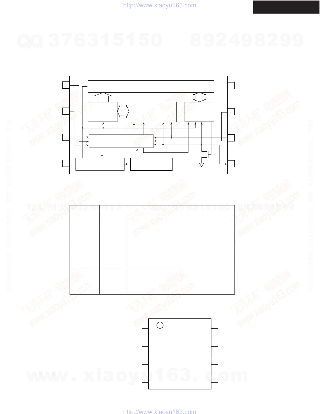
Q8201: BR24S32FJ(32kbit, 4096x8 bit EEPROM)
BLOCK DIAGRAM AND PIN CONFIGURATION
TERMINAL DESCRIPTION
PIN LAYOUT
IC BLOCK DIAGRAMS AND TERMINAL DESCRIPTIONS -57
TX-SR806/SA806
1
2
3
4
8
7
6
5
Vcc
WP
SCL
SDA
A0
A1
A2
GND
Terminal
Name
Vcc
GND
A0,A1,A2
SCL
SDA
WP
I/O
-
-
I
I
I/O
I
Function
Connect the power source
Reference voltage of all input / output, 0V
Slave address setting terminal
Serial clock input
Slave and word address
Serial data input, serial data output
Write protect terminal
SOP-J8
w
w
w
.
x
i
a
o
y
u
1
6
3
.
c
o
m
Q
Q
3
7
6
3
1
5
1
5
0
9
9
2
8
9
4
2
9
8
T
E
L
1
3
9
4
2
2
9
6
5
1
3
9
9
2
8
9
4
2
9
8
0
5
1
5
1
3
6
7
3
Q
Q
TEL 13942296513 QQ 376315150 892498299
TEL 13942296513 QQ 376315150 892498299
http://www.xiaoyu163.com
http://www.xiaoyu163.com
 Loading...