21555 Non-Transparent PCI-to-PCI Bridge User Manual 155
List of Registers
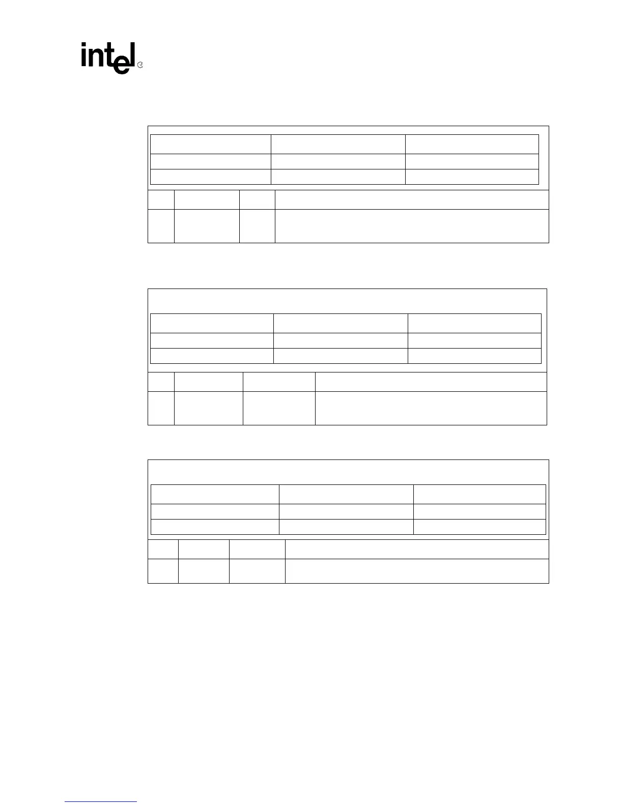
Table 73. Primary and Secondary Interrupt Pin Registers
Bit Name R/W Description
7:0 Interrupt Pin R
This register indicates which PCI interrupt pin the 21555 uses on the
corresponding bus. This is a read
-only register and always returns 1 when
read indicating that the 21555 uses INTA#.
Table 74. Primary and Secondary Minimum Grant Registers
These registers may be preloaded through the serial ROM. The Primary Minimum Grant register may also be
programmed by the local processor.
Bit Name R/W Description
7:0 MIN_GNT (MG)
PMG: R/(WS)
SMG: R
Specifies how long of a burst period the 21555 needs on the
corresponding bus in units of 1/4
µsec. Reads as 0 before
preload.
Table 75. Primary and Secondary Maximum Latency Registers
These registers may be preloaded through the serial ROM. The Primary Maximum Latency register may also be
programmed by the local processor
.
Bit Name R/W Description
7:0
MAX_LAT
(ML)
PML: R/(WS)
SML: R
Specifies how often the 21555 needs to gain access to the
corresponding bus in units of 1/4
µsec. Reads as 0 before preload.
Offsets Primary Interrupt Pin Secondary Interrupt Pin
Primary byte 3Dh 7Dh
Secondary byte 7Dh 3Dh
Offsets Primary Minimum Grant Secondary Minimum Grant
Primary byte 3Eh 7Eh
Secondary byte 7Eh 3Eh
Offsets Primary Maximum Latency Secondary Maximum Latency
Primary byte 3Fh 7Fh
Secondary byte 7Fh 3Fh