21555 Non-Transparent PCI-to-PCI Bridge User Manual 141
List of Registers
.
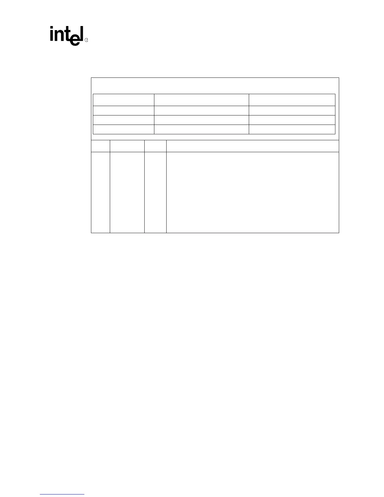
Table 46. Downstream and Upstream Configuration Address Registers
This section describes both the downstream and upstream versions of the registers. These
registers are also mapped in memory and I/O space.
Bit Name R/W Description
31:0
CFG_ADDR
(CA)
DCA:
R/(WP)
UCA:
R/(WS)
This register contains the address for a configuration transaction to be
generated on the target bus. The address is driven exactly as written in this
register. This register should be written before the corresponding
Downstream or Upstream Configuration Data register is accessed. Once
the Downstream or Upstream Configuration Data register is accessed, the
transaction is initiated on the secondary or primary bus, respectively. When
the semaphore method is used, a master should not write to this register
unless the master has successfully read a 0 from the Downstream or
Upstream Configuration Own bit.
The Downstream Configuration Address register cannot be written from the
secondary interface.
The Upstream Configuration Address register cannot be written from the
primary interface.
Offsets Downstream Configuration Address Upstream Configuration Address
Primary byte 83:80h 8B:88h (Reserved)
Secondary byte 83:80h (Reserved) 8B:88h
CSR Space 003:000h 00B:008h