Intel Desktop Board D915GAV/D915GAG Technical Product Specification
18
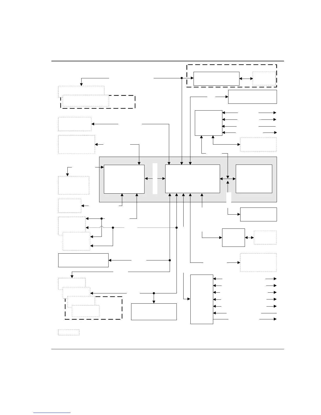
1.3.4 Block Diagram
Figure 3 is a block diagram of the major functional areas of the boards.
D915GAG only
D915GAV
only
Intel 915G Chipset
Intel 82801FB
I/O Controller Hub
(ICH6)
Intel 82915G
Graphics and
Memory Controller
Hub (GMCH)
4 Mbit
Firmware Hub
(FWH)
System Bus
(800/533 MHz)
LGA775
Processor Socket
Parallel ATA
IDE Connector
Diskette Drive
Connector
LPC Bus
I/O
Controller
PS/2 Keyboard
PS/2 Mouse
Parallel Port
Serial Ports
Parallel ATA
IDE Interface
LPC Bus
Hardware Monitoring
and Fan Control ASIC
OM17551
Audio
Codec
Retasking Jack F [Port 2]
Line Out/Retasking Jack D
CD-ROM (optional)
Retasking Jack E [Port 1]
LAN
Connector
10/100
LAN PLC
(Optional)
PCI Express
x16 Interface
PCI Express
x16
Connector
= connector or socket
PCI Bus
SMBus
High Definition Audio Link
USB
Dual-Channel
Memory Bus
SMBus
PCI Slot 1
PCI Slot 2
PCI Slot 3
PCI Slot 4
Mic In/Retasking Jack B
Line In/Retasking Jack C
S/PDIF (optional)
Serial ATA IDE
Connectors (4)
Serial ATA
IDE Interface
VGA
Port
Display Interface
Channel A
DIMMs (2)
Channel B
DIMMs (2)
Back Panel/Front Panel
USB Ports
DMI Interconnect
PCI Bus
TPM Component
(Optional)
LPC Bus
IEEE-1394a Connectors
(Optional)
LAN Connect
Interface
D915GAV
only
PCI Express x1 Slot 1
PCI Express x1 Slot 2
PCI Express x1 Interface
LAN
Connector
Gigabit Ethernet
Controller (Optional)
Figure 3. Block Diagram