Contents
ix
Figures
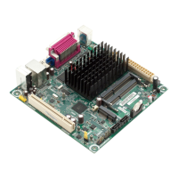
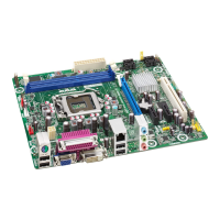
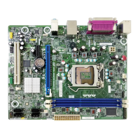
1. Major Board Components .................................................................. 13
2. Block Diagram .................................................................................. 15
3. LAN Connector LED Locations ............................................................. 24
4. Back Panel Audio Connectors ............................................................. 26
5. Thermal Sensors and Fan Header ....................................................... 28
6. Location of the Standby Power Indicator LED ....................................... 34
7. Detailed System Memory Address Map ................................................ 36
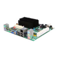
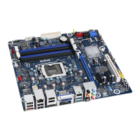
8. Back Panel Connectors ...................................................................... 39
9. I/O Shield Reference Diagram ............................................................ 40
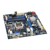
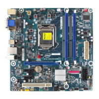
10. Component-side Connectors and Headers ............................................ 41
11. Connection Diagram for Front Panel Header ......................................... 48
12. Connection Diagram for Front Panel USB Header .................................. 50
13. Connection Diagram for Front Panel USB Header with
Intel Z- USB Solid-State Drive or Compatible Device Support ................. 50
14. Location of the BIOS Configuration Jumper Block .................................. 51
15. Board Dimensions ............................................................................. 53
16. Localized High Temperature Zones ..................................................... 55
17. Fan Location Guide for Cassis Selection (Chassis Orientation is
Not Restricted) ................................................................................. 58
Tables
1. Feature Summary ............................................................................. 11
2. Board Components Shown in Figure 1 ................................................. 14
3. Supported Memory Configurations ...................................................... 18
4. LAN Connector LED States ................................................................. 24
5. Audio Jack Support ........................................................................... 25
6. Effects of Pressing the Power Switch ................................................... 29
7. Power States and Targeted System Power ........................................... 30
8. Wake-up Devices and Events ............................................................. 31
9. System Memory Map ........................................................................ 37
1
0. Component-side Connectors and Headers Shown in Figure 10 ................ 42
11. Serial Port Header ............................................................................ 43
12. LVDS Data Connector - 30-Pin (D525MWV only) ................................... 43
13. LVDS Panel Voltage Selection Jumper (D525MWV only) ......................... 44
14. LVDS Inverter Power Connector (D525MWV only) ................................. 44
15. LVDS Inverter Power Voltage Selection Jumper (D525MWV only) ........... 44
16. Chassis Fan Header .......................................................................... 44
17. SATA Connectors .............................................................................. 45
18. Front Panel Wireless Activity LED Header ............................................. 45
19. Front Panel Audio Header for Intel HD Audio ........................................ 45
20. Front Panel Audio Header for AC ’97 Audio ........................................... 45
21. Front Panel USB Header .................................................................... 46