Detailed Function Description
67
Figure 6.18 FDT level and lag diagram.
Function
Code
Name Description
Setting
Range
Factory
Setting
P8.15
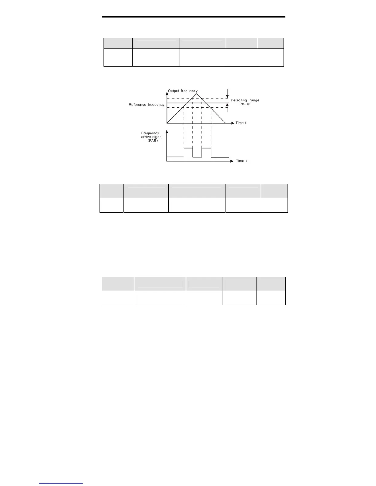
Frequency arrive
detecting range
0.0~100.0%
(maximum
frequency)
0.0~100.0 0.0%
When output frequency is within the detecting range of reference frequency, an ON-OFF
signal will be output.
Figure 6.19 Frequency arriving signal diagram.
Function
Code
Name Description Setting Range
Factory
Setting
P8.16
Brake threshold
voltage
115.0~140.0% 115.0~140.0
Depend
on model
When the DC bus voltage is greater than the value of P8.16, the inverter will start
dynamic braking.
Notice:
Factory setting is 120% if rated voltage of inverter is 220V.
Factory setting is 130% if rated voltage of inverter is 380V.
The value of P8.16 is corresponding to the DC bus voltage at rated input
voltage.
Function
Code
Name Description
Setting
Range
Default
Value
P8.17
Coefficient of rotation
speed
0.1~999.9% 0.1~999.9% 100.0%
 Loading...