Philips Semiconductors Product specification
Multiple voltage regulator with switch and
ignition buffer
TDA3681
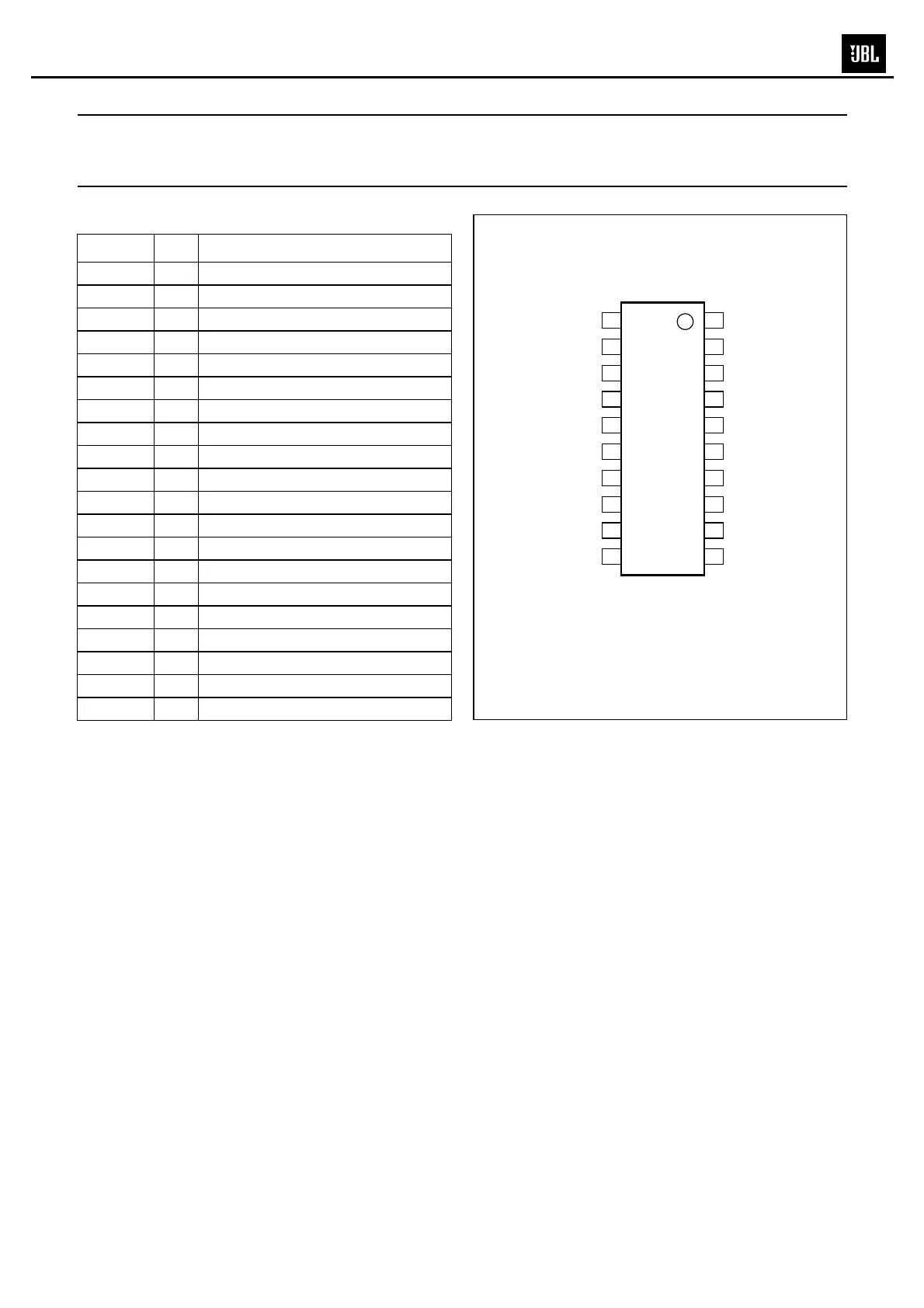
Pin description of TDA3681TH
Note
1. The pin is used for final test purposes. In the
application it should be connected directly to ground.
SYMBOL PIN DESCRIPTION
REG4 1 regulator 4 output
IGN
IN
2 ignition input
IGN
OUT
3 ignition output (active HIGH)
RES 4 reset output (active LOW)
C
RES
5 reset delay capacitor
EN4 6 enable input for regulator 4
EN1/3 7 enable input for regulators 1 and 3
ENSW 8 enable input for power switch
HOLD 9 hold output (active LOW)
GND 10 ground
HEATTAB 11 heat tab connection; note 1
REG2 12 regulator 2 output
BU 13 backup switch output
V
P1
14 supply voltage
n.c. 15 not connected
SW 16 power switch output
REG1 17 regulator 1 output
n.c. 18 not connected
REG3 19 regulator 3 output
V
P2
20 second supply voltage
handbook, halfpage
TDA3681TH
MGU329
1
2
3
4
5
6
7
8
9
10
REG4
IGN
IN
IGN
OUT
RES
C
RES
EN4
EN1/3
ENSW
HOLD
GND
V
P2
REG3
n.c.
REG1
SW
n.c.
V
P1
BU
REG2
HEATTAB
20
19
18
17
16
15
14
13
12
11
Fig.4 Pin configuration for TDA3681TH.
MS-8