Philips Semiconductors Product specification
Multiple voltage regulator with switch and
ignition buffer
TDA3681
PINNING
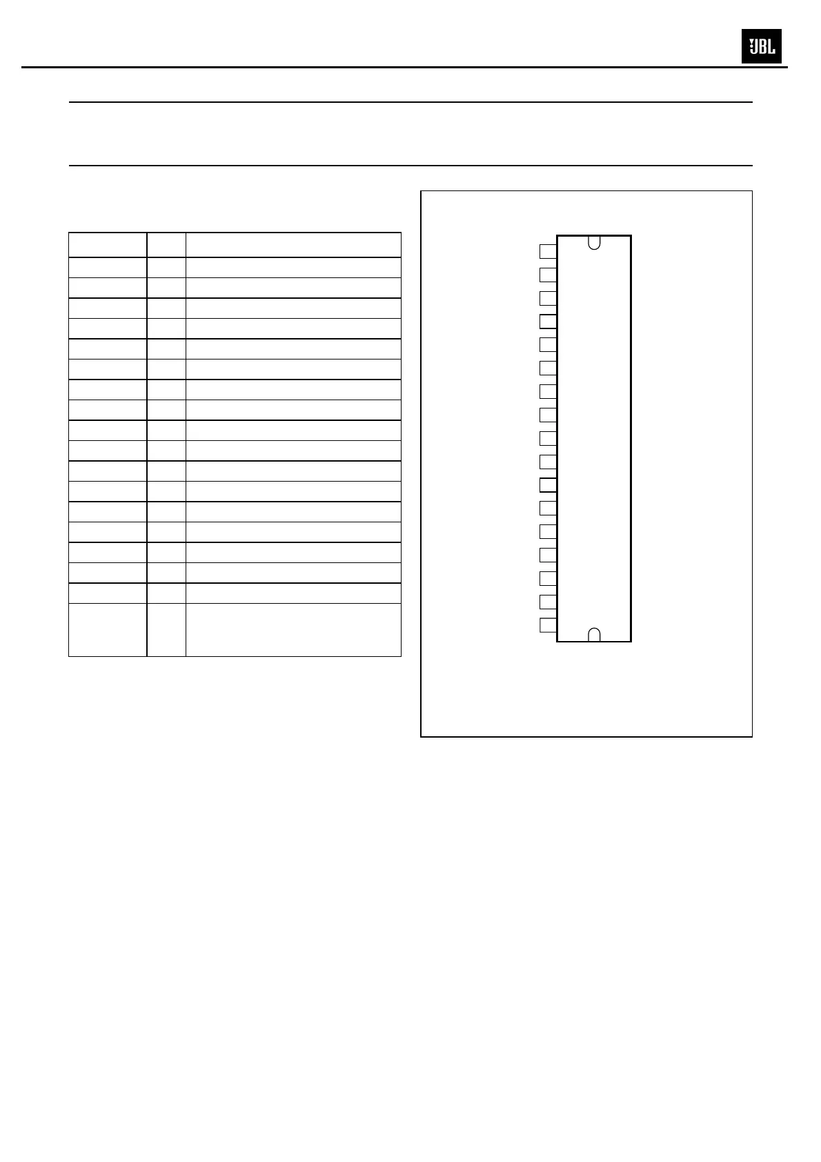
Pin description of TDA3681J and TDA3681JR
SYMBOL PIN DESCRIPTION
REG1 1 regulator 1 output
REG3 2 regulator 3 output
V
P2
3 second supply voltage
REG4 4 regulator 4 output
IGN
IN
5 ignition input
IGN
OUT
6 ignition output (active HIGH)
RES 7 reset output (active LOW)
C
RES
8 reset delay capacitor
EN4 9 enable input for regulator 4
EN1/3 10 enable input for regulators 1 and 3
ENSW 11 enable input for power switch
HOLD 12 hold output (active LOW)
GND 13 ground
BU 14 backup switch output
REG2 15 regulator 2 output
SW 16 power switch output
V
P1
17 supply voltage
heat tab − heat tab; it is strongly
recommended to connect the heat
tab to ground
handbook, halfpage
TDA3681J
TDA3681JR
MGL903
V
P2
REG1
REG3
REG4
IGN
IN
IGN
OUT
C
RES
EN4
RES
EN1/3
ENSW
HOLD
GND
BU
REG2
SW
V
P1
1
2
3
4
5
6
7
8
9
10
11
12
13
14
15
16
17
Fig.3 Pin configuration for TDA3681J and
TDA3681JR.
MS-8