Part No. 960-000187R_Rev. A © 2016 JCM American Corporation
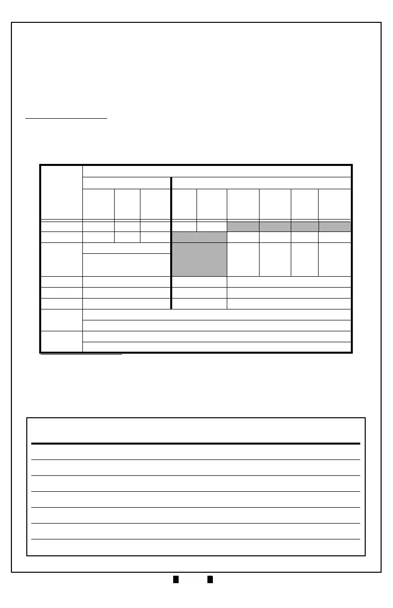
Table 3 lists the default Configuration Settings for DIP Switch Block #2.
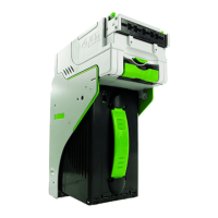
– Photo-Coupler (9600 bps) – Pulse
– TTL (38400 bps) – USB 2.0*
* USB Communications requires an external harness for USB connection.
– RS-232C (38400 bps)
Table 3 DIP Switch Block #2 Configuration Settings (Default)
Switch
No.
DIP Switch #2*
* For correct DIP Switch Block #2 Settings for other protocols, check the Software Information
Sheet (SIS) for the specific protocol.
ID-003 ID-0E4
Photo
Coupler
TTL
RS-
232C
TTL
RS-
232C
Baud
Rate
9600
bps
Baud
Rate
19200
bps
Baud
Rate
38400
bps
Baud
Rate
115200
bps
1 OFF ON OFF OFF ON
2OFFOFFON OFF ON OFF ON
3
OFF = Standard ID-003
OFF OFF ON ON
ON = Send Enable or
Disable Status before
Stacker Full
4 OFF OFF OFF
5 OFF OFF OFF
6 OFF OFF OFF
7
OFF = Standard Current Mode [Peak Current: 3.0A]
ON = Maximum Current Limitation Mode [Peak Current: 2.0A]
8
OFF = ID-003 Mode
ON = ID-0E4 Mode