TOS7200 43
SIGNAL I/O Connector
Specifications for the SIGNAL I/O connector
Input signal
Low-active control input
Active LOW control input: 11 V to 15 V
High-level input voltage: 0 V to 4 V
Low-level input voltage: -5 mA maximum
Input time width: 5 ms minimum
Output signal
Open drain output
Output withstand voltage: 30 Vdc
Output saturation voltage: Approx. 0.7 V (25 °C)
Maximum output current: 400 mA (TOTAL)
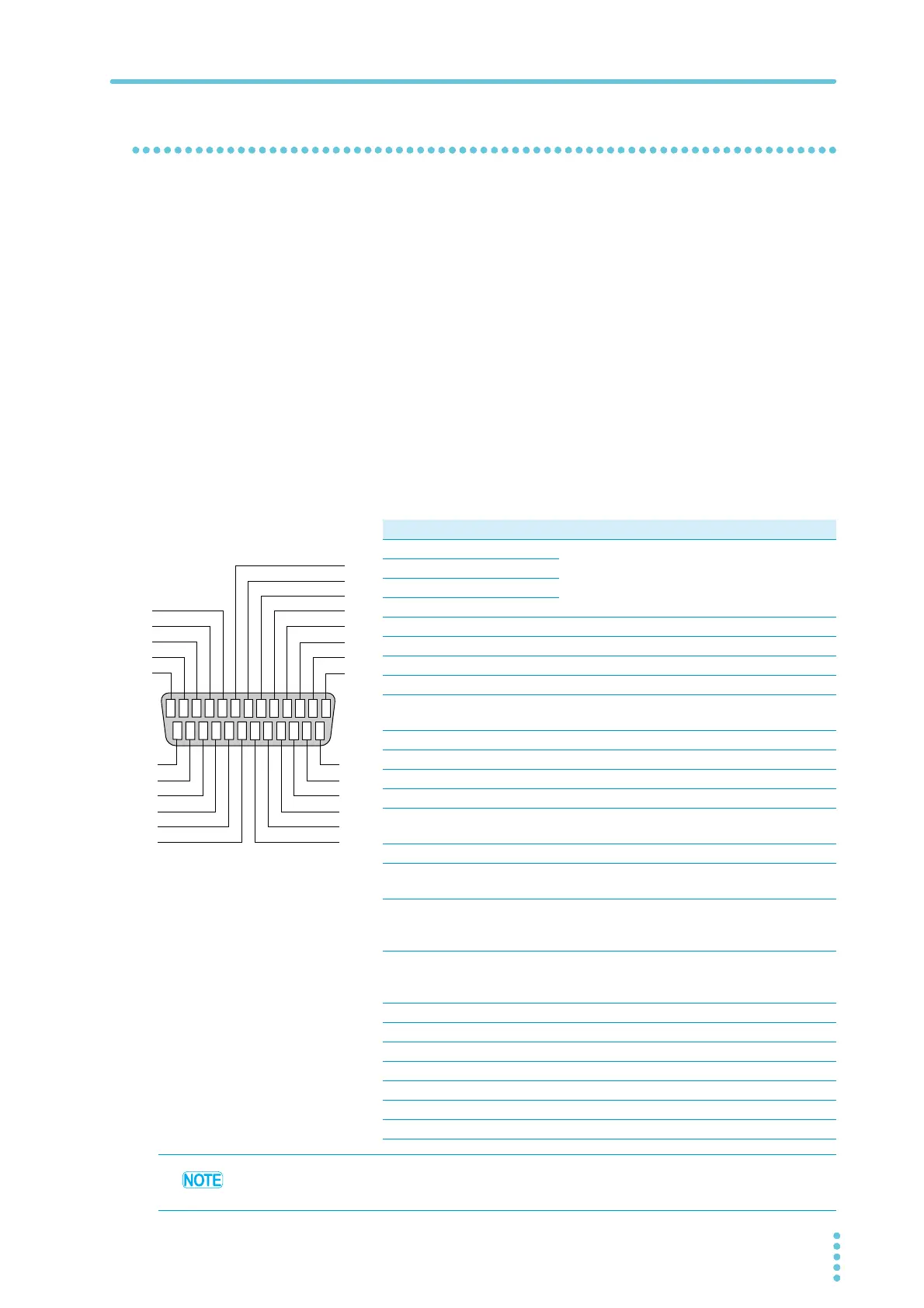
Pin assignment
No. Signal name I/O Description of signal
1 PM0 I LSB 1-digit BCD active LOW input
Panel memory’s selection signal input terminal
2PM1 I
3PM2 I
4PM3 I MSB
5N.C
6N.C
7N.C
8N.C
9 STB I Input terminal for the strobe signal of the panel
memory
10 N.C
11 N.C
12 N.C
13 COM Circuit common (chassis potential)
14 HV ON O ON during a test or while a voltage remains between
the output terminals
15 TEST O ON during a test
16 PASS O ON for approx. 0.2 seconds when PASS judgment is
made, or continuously ON while PASS HOLD is activated
17 U FAIL O Continuously ON if an insulation resistance equal to or
exceeding the upper resistance is detected, resulting in
FAIL judgment
18 L FAIL O Continuously ON if an insulation resistance equal to or
falling below the lower resistance is detected, resulting
in FAIL judgment
19 READY O ON during standby
20 N.C
21 START I Input terminal for the START signal
22 STOP I Input terminal for the STOP signal
23 ENABLE I Remote control enable signal input terminal
24 N.C
25 COM Circuit common (chassis potential)
Input signals cannot be directly controlled using logic IC such as HC.
987654321
13 12 11 10
19 18 17 16 15 1424 23 22 21 2025
Pin Configuration for the SIGNAL I/O Connector
 Loading...