54 TOS7200
Specifications
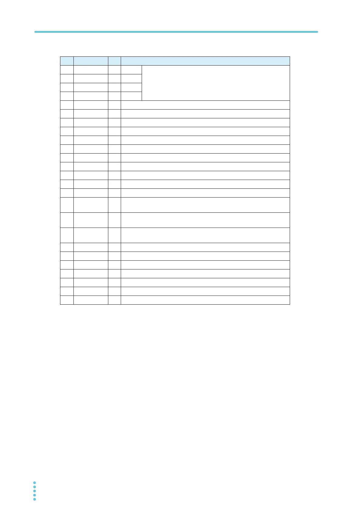
Table.3 SIGNAL I/O pin assignment
No. Signal name I/O Description of signal
1 PM0 I LSB 1-digit BCD active LOW input
Panel memory’s selection signal input terminal
2PM1I
3PM2I
4PM3IMSB
5N.C
6N.C
7N.C
8N.C
9 STB I Input terminal for the strobe signal of the panel memory
10 N.C
11 N.C
12 N.C
13 COM Circuit common (chassis potential)
14 HV ON O ON during a test or while a voltage remains between the output terminals
15 TEST O ON during a test
16 PASS O ON for approx. 0.2 seconds when PASS judgment is made, or continuously ON
while PASS HOLD is activated
17 U FAIL O Continuously ON if an insulation resistance equal to or exceeding the upper
resistance is detected, resulting in FAIL judgment
18 L FAIL O Continuously ON if an insulation resistance equal to or falling below the lower
resistance is detected, resulting in FAIL judgment
19 READY O ON during standby
20 N.C
21 START I Input terminal for the START signal
22 STOP I Input terminal for the STOP signal
23 ENABLE I Remote control enable signal input terminal
24 N.C
25 COM Circuit common (chassis potential)


 To Next Page