iCE40 Ultra Breakout Board
Evaluation Board User Guide
© 2014-2020 Lattice Semiconductor Corp. All Lattice trademarks, registered trademarks, patents, and disclaimers are as listed at www.latticesemi.com/legal.
All other brand or product names are trademarks or registered trademarks of their respective holders. The specifications and information herein are subject to change without notice.
10 FPGA-EB-02034-1.2
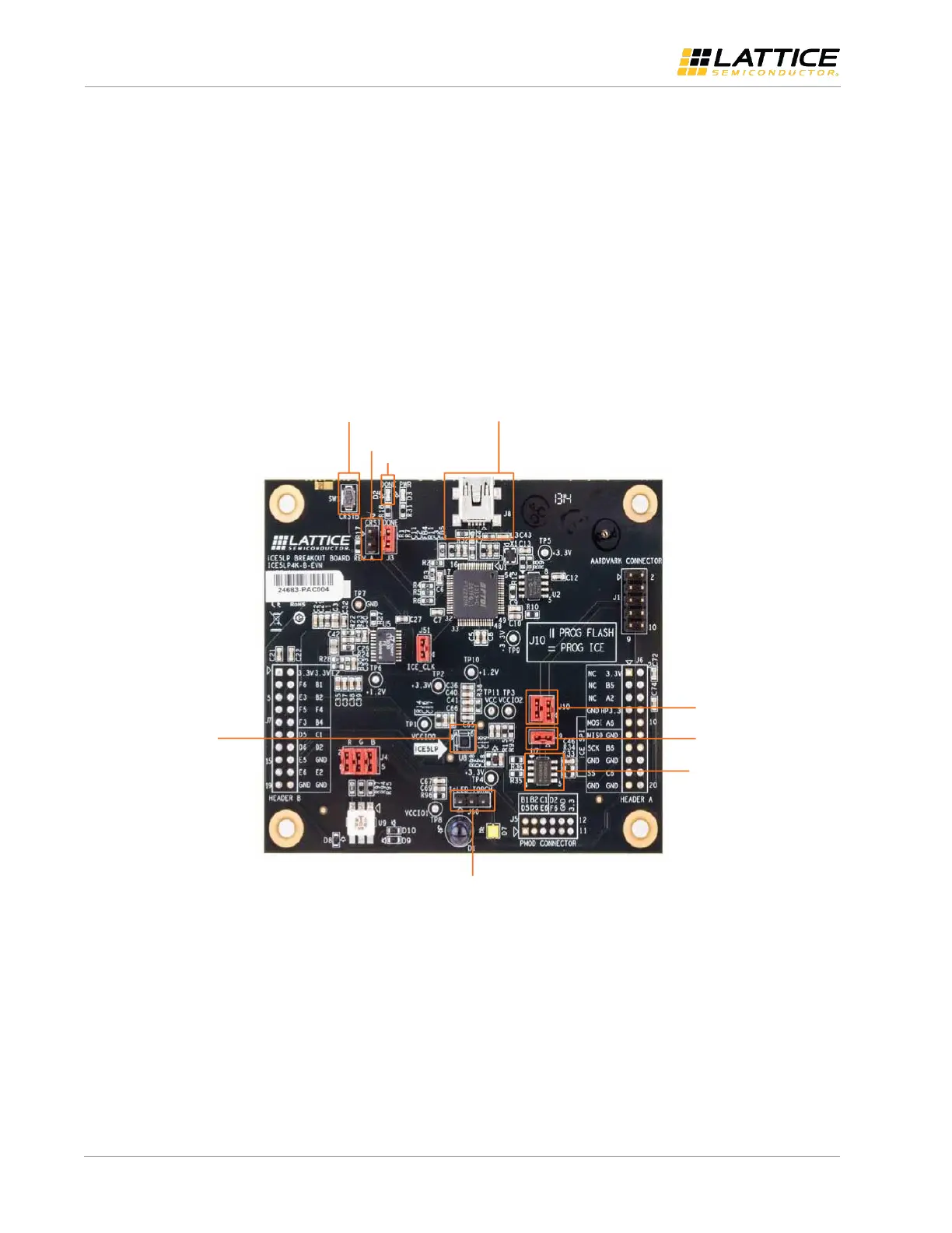
8. Board Configuration and Programming
The board allows for programming of the iCE40 Ultra or the SPI Flash:
SPI Flash Programming J10 shunt pins 1-3 and 2-4 (default shunted)
U7 Micron Technology Inc part number N25Q032A13ESC40F
iCE40 Ultra Configuration or Programming J10 shunt pins 1-2 and 3-4
U8 iCE5LP4K-SWG36
CRESETB can be asserted by pushing SW1.
Can be probed with J2
Done LED D2
Can be probed with J3 (default shunted)
Details of the iCE40 Ultra Board for use in programming are shown in Figure 8.1.
CRESETB
Push-Button
USB Interface
Socket
J2 – CRESETB Probe
D2 – DONE LED
J50 – Selects HP LED
Device (IR or Torch)
U8 –
iCE5LP4K – SWG36
J10 – Program
SPI Flash or iCE5LP
J9 – Isolate
SPI Flash CSn
U7 –
N25Q032A13ESC40F
Figure 8.1. Configuration and Programming Details