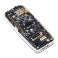
iCE40 Ultra Breakout Board
Evaluation Board User Guide
© 2014-2020 Lattice Semiconductor Corp. All Lattice trademarks, registered trademarks, patents, and disclaimers are as listed at www.latticesemi.com/legal.
All other brand or product names are trademarks or registered trademarks of their respective holders. The specifications and information herein are subject to change without notice.
FPGA-EB-02034-1.2 9
6. Clock Sources
The board has a single 12 MHz clock source. The 12 MHz clock drives both the FTDI USB interface device and the
iCE5LP4K device. The iCE5LP4K can be disconnected from the 12 MHz oscillator using J51. This is necessary, for
example, when iCE40 Ultra device ball C2 is mistakenly programmed as an output and prevents the FTDI USB interface
from operating.
7. Board Power
The board provides the following power features:
Board Power
Board power is derived from the USB connection.
D3 Green LED indicates Board Power.
iCE40 Ultra VCC
Onboard 1.2 V supply
ICC can be measured across the series resistor R38 (1 Ω) at TP10 and TP11.
iCE40 Ultra VCCIO
Onboard 3.3 V supply
ICC0 can be measured across the series resistor R14 (1 Ω) at TP1 and TP2.
ICC1 can be measured across the series resistor R96 (1 Ω) at TP8 and TP9.
ICC2 can be measured across the series resistor R15 (1 Ω) at TP3 and TP4.
The power supplies on the iCE40 Ultra Breakout Board are simplified and suitable for booting from the external SPI
flash. The power supply sequencing does not conform to the NVCM boot requirements as specified in iCE40 Ultra
Family Data Sheet (FPGA-DS-02028). You may encounter intermittent boot success and/or higher than specified startup
currents when attempting to boot from NVCM.
There are two versions of the BOM. Early versions have D6 populated with a CDBU0520 Schottky. Later versions
populate D6 with a CDSU4148. The later version diode complies with the voltage requirements on the Vpp_2V5 pin for
NVCM programming/configuration.