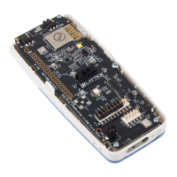
iCE40 Ultra Breakout Board
Evaluation Board User Guide
© 2014-2020 Lattice Semiconductor Corp. All Lattice trademarks, registered trademarks, patents, and disclaimers are as listed at www.latticesemi.com/legal.
All other brand or product names are trademarks or registered trademarks of their respective holders. The specifications and information herein are subject to change without notice.
20 FPGA-EB-02034-1.2
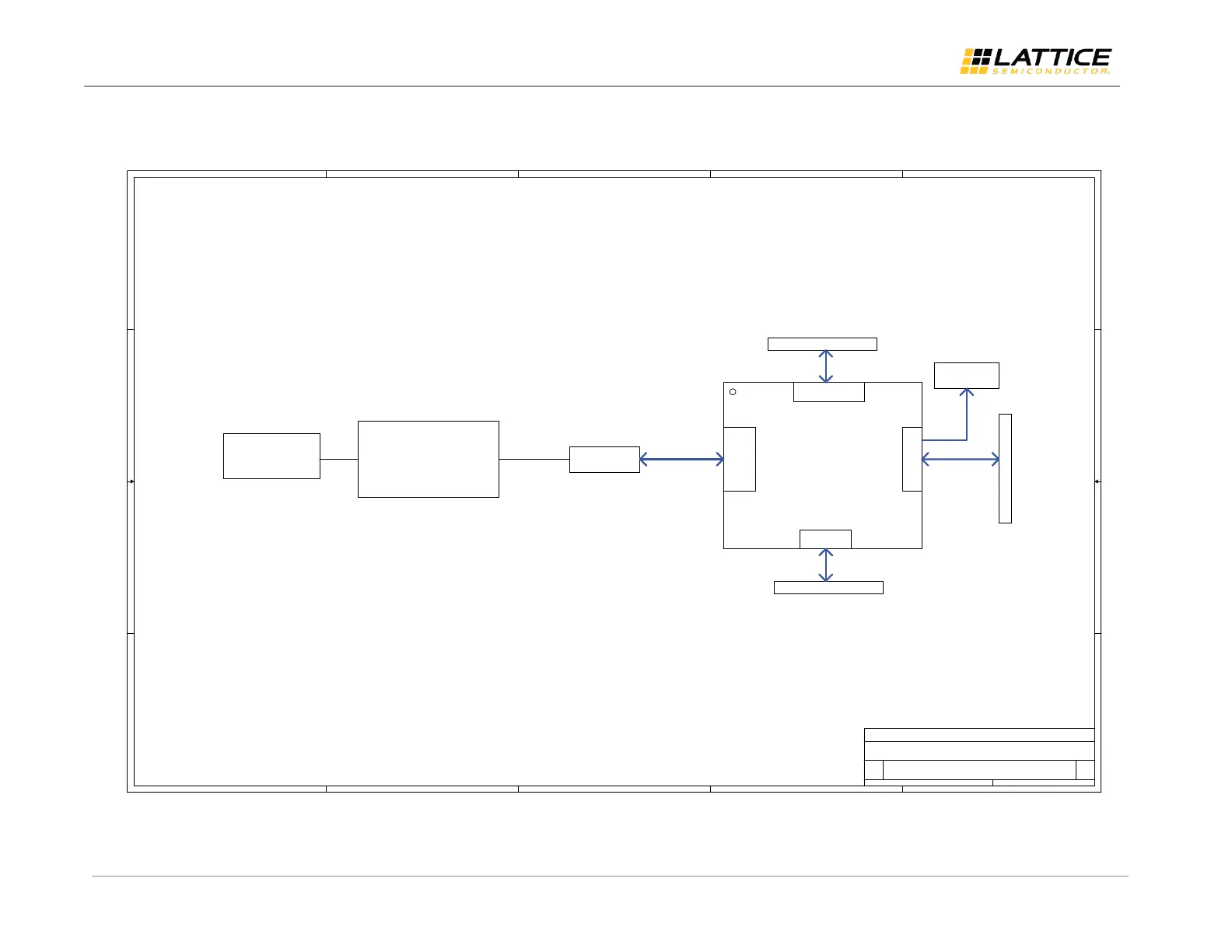
Appendix A. Schematic Diagrams
Figure A.1. Block Diagram
5
4
3
2
1
D
C
B
A
FPGA
Power from USB 5V
SPI
BANK 0
BANK 1
BANK 2
iCE5LP4KSWG36
HEADER B
HEADER B
HEADER A
I/O
I/O
I/O
USB
CONNECTOR
USB to
SPI / RS232
LEDS
BLOCK DIAGRAM
iCE40 Ultra BREAKOUT BOARD
BLOCK DIAGRAM
SPI
Page : 3
Page : 6
Aardvark Connector
Page : 7
BANK 1
Page : 4
Page : 5
Title
Size Document Number Rev
Date: Sheet
of
<Doc> AB
27Thursday, March 06, 2014
Title
Size Document Number Rev
Date: Sheet
of
<Doc> AB
27Thursday, March 06, 2014
Title
Size Document Number Rev
Date: Sheet
of
<Doc> AB
27Thursday, March 06, 2014

 Loading...