iCE40 Ultra Breakout Board
Evaluation Board User Guide
© 2014-2020 Lattice Semiconductor Corp. All Lattice trademarks, registered trademarks, patents, and disclaimers are as listed at www.latticesemi.com/legal.
All other brand or product names are trademarks or registered trademarks of their respective holders. The specifications and information herein are subject to change without notice.
FPGA-EB-02034-1.2 15
11. User Interface Serial Communication Interface
11.1. LED Control through SPI
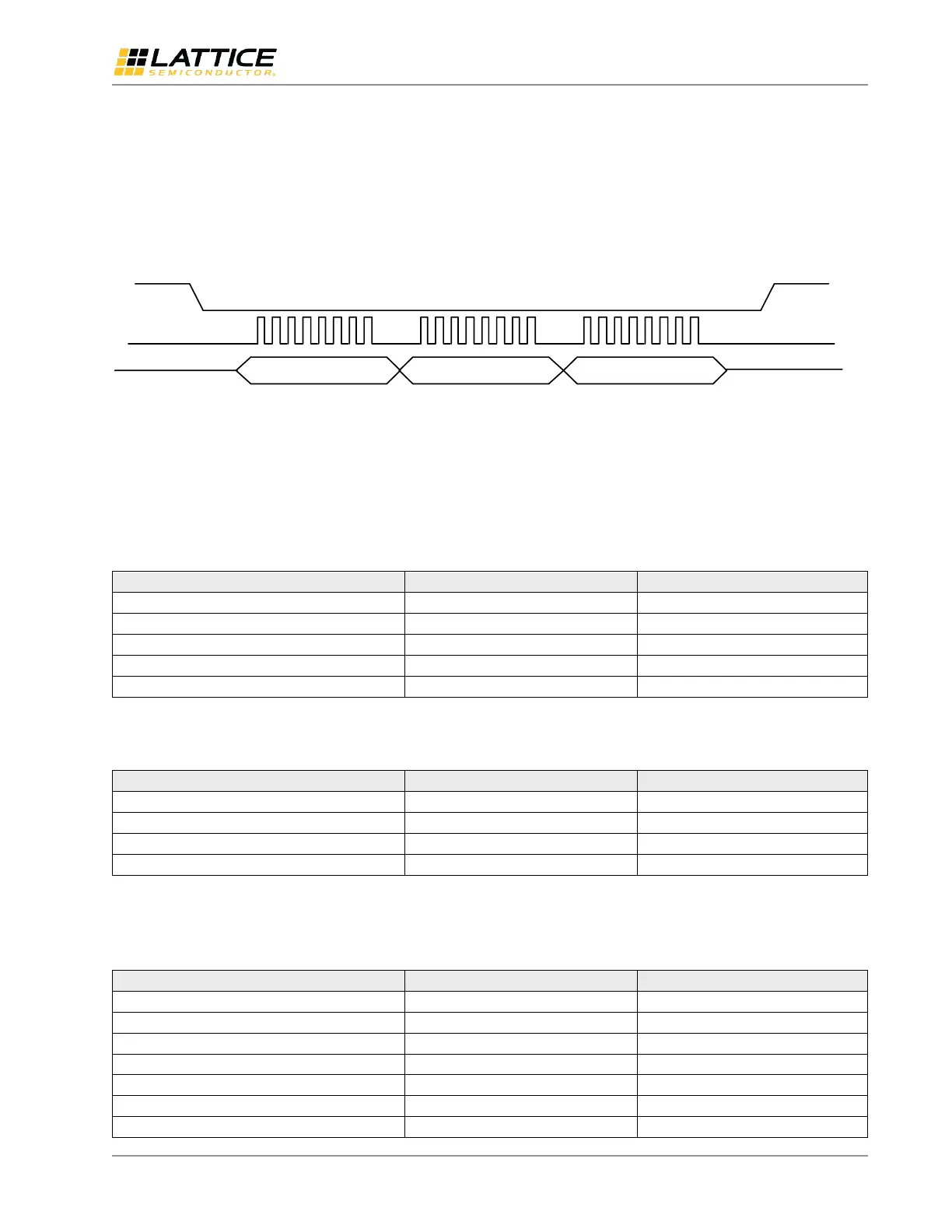
The software user interface demonstration program communicates with the iCE40 Ultra device using an SPI serial
communication channel. The SPI interface (mode 0) control link is implemented using a simple write-only protocol (see
Figure 11.1).
CSn
SCK
MOSI
ADDR [7:0] REG [15:8] REG [7:0]
Figure 11.1. SPI Physical Transaction
11.2. SPI Protocol
Data on the MOSI serial line is transmitted MSB first. Addr[7:0] – Controls which of the 16 bits are updated with REG
data.
Note: Unspecified REG bits must be written, but are ignored.
Table 11.1. ADDR [7:0]
REG[15:0] – Consists of four control fields.
Table 11.2. REG [15:0]
11.3. Register Definitions
Table 11.3. RGB Color [3:0]


 To Next Page