iCE40 Ultra Breakout Board
Evaluation Board User Guide
© 2014-2020 Lattice Semiconductor Corp. All Lattice trademarks, registered trademarks, patents, and disclaimers are as listed at www.latticesemi.com/legal.
All other brand or product names are trademarks or registered trademarks of their respective holders. The specifications and information herein are subject to change without notice.
4 FPGA-EB-02034-1.2
Figures
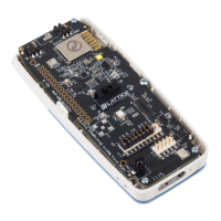
Figure 2.1. Top Side of the iCE40 Ultra Breakout Board ....................................................................................................... 7
Figure 5.1. Default Shunt Locations ...................................................................................................................................... 8
Figure 8.1. Configuration and Programming Details .......................................................................................................... 10
Figure 9.1. J6 Header A Breakouts ...................................................................................................................................... 11
Figure 9.2. J7 Header B Breakouts ...................................................................................................................................... 11
Figure 9.3. J5 PMOD Connector .......................................................................................................................................... 11
Figure 9.4. J7 Header B Breakouts ...................................................................................................................................... 12
Figure 9.5. Breakout Headers ............................................................................................................................................. 12
Figure 10.1. SPI Flash Selection for J10 (Vertical) ............................................................................................................... 13
Figure 10.2. iCE40 Ultra Selection for J10 (Horizontal) ....................................................................................................... 13
Figure 10.3. iCE40 Ultra LED Demonstration Interface ....................................................................................................... 14
Figure 11.1. SPI Physical Transaction .................................................................................................................................. 15
Figure A.1. Block Diagram ................................................................................................................................................... 20
Figure A.2. FTDI Connection ............................................................................................................................................... 21
Figure A.3. DUT Connection ................................................................................................................................................ 22
Figure A.4. LEDs and Headers ............................................................................................................................................. 23
Figure A.5. Regulator Connection ....................................................................................................................................... 24
Figure A.6. SPI ..................................................................................................................................................................... 25
Tables
Table 11.1. ADDR [7:0] ........................................................................................................................................................ 15
Table 11.2. REG [15:0] ........................................................................................................................................................ 15
Table 11.3. RGB Color [3:0] ................................................................................................................................................. 15
Table 11.4. Brightness [3:0] ................................................................................................................................................ 16
Table 11.5. Breathe Ramp [3:0] .......................................................................................................................................... 16
Table 11.6. Blink Rate [3:0] ................................................................................................................................................. 17
Table 12.1. Ordering Information ....................................................................................................................................... 18