MT41K128M16JT-125:K (DIGITAL : U104, U254)
Block Diagram
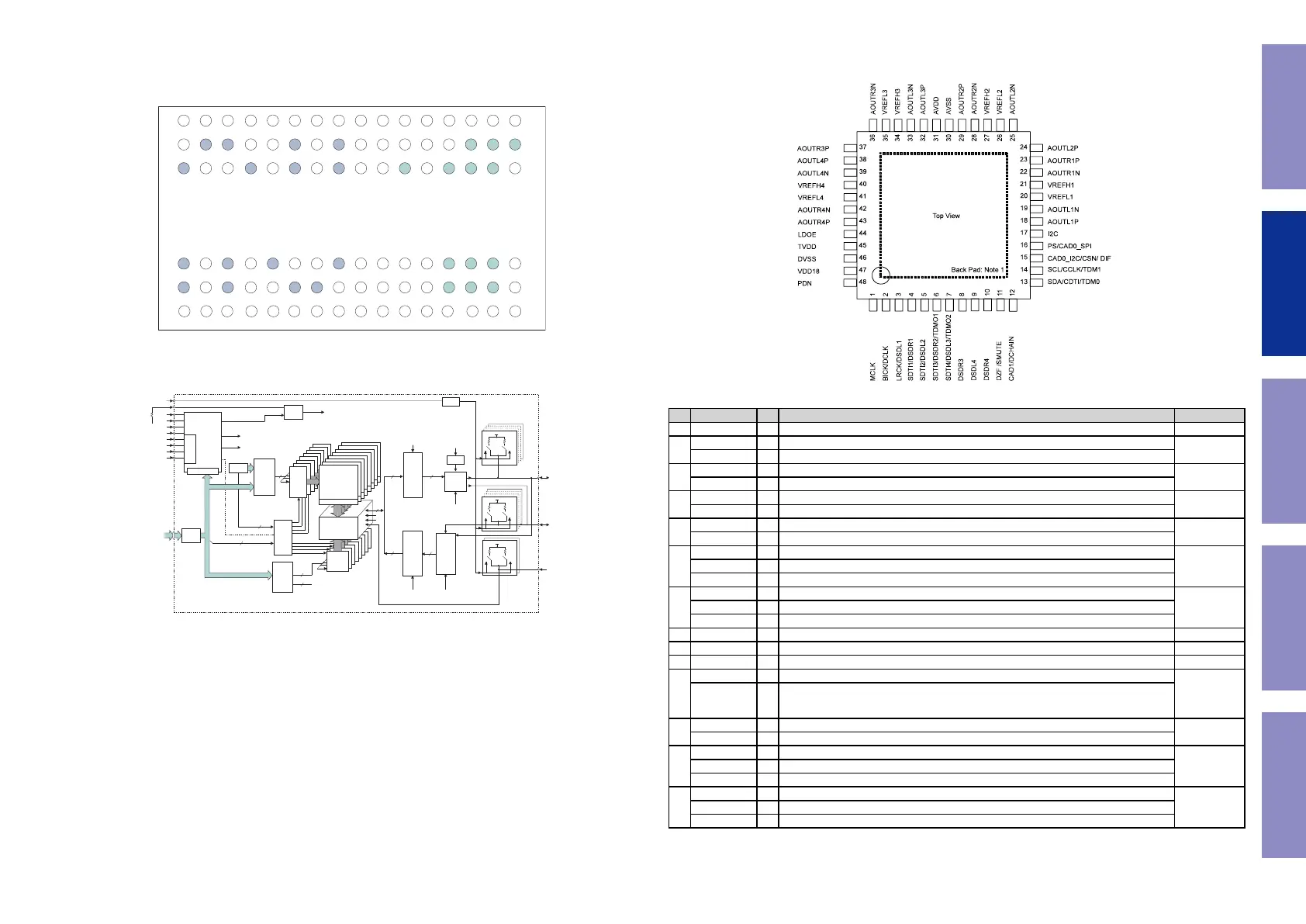
Figure 7: 96-Ball FBGA – x16 Ball Assignments (Top View)
1234 67895
A
B
C
D
E
F
G
H
J
K
L
M
N
P
R
T
V
DDQ
V
SSQ
V
DDQ
V
SSQ
V
SS
V
DDQ
V
SSQ
V
REFDQ
NC
ODT
NC
V
SS
V
DD
V
SS
V
DD
V
SS
DQ13
V
DD
DQ11
V
DDQ
V
SSQ
DQ2
DQ6
V
DDQ
V
SS
V
DD
CS#
BA0
A3
A5
A7
RESET#
DQ15
V
SS
DQ9
UDM
DQ0
LDQS
LDQS#
DQ4
RAS#
CAS#
WE#
BA2
A0
A2
A9
A13
DQ12
UDQS#
UDQS
DQ8
LDM
DQ1
V
DD
DQ7
CK
CK#
A10/AP
NC
A12/BC#
A1
A11
NC
V
DDQ
DQ14
DQ10
V
SSQ
V
SSQ
DQ3
V
SS
DQ5
V
SS
V
DD
ZQ
V
REFCA
BA1
A4
A6
A8
V
SS
V
SSQ
V
DDQ
V
DD
V
DDQ
V
SSQ
V
SSQ
V
DDQ
NC
CKE
NC
V
SS
V
DD
V
SS
V
DD
V
SS
Notes:
1. Ball descriptions listed in Table 4 (page 20) are listed as “x16.”
2. A comma separates the configuration; a slash defines a selectable function.
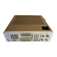
Figure 5: 128 Meg x 16 Functional Block Diagram
Bank 5
Bank 6
Bank 7
Bank 4
Bank 7
Bank 4
Bank 5
Bank 6
13
Row-
address
MUX
Control
logic
Column-
address
counter/
latch
Mode registers
10
Command
decode
A[13:0]
BA[2:0]
14
Address
register
17
(128
x128)
16,384
I/O gating
DM mask logic
Column
decoder
Bank 0
memory
array
(16,384 x 128 x 128)
Bank 0
row-
address
latch
and
decoder
16,384
Sense amplifiers
Bank
control
logic
17
Bank 1
Bank 2
Bank 3
14
7
3
3
Refresh
counter
16
128
128
128
LDQS, LDQS#, UDQS, UDQS#
Column 0, 1, and 2
Columns 0, 1, and 2
ZQCL, ZQCS
To ODT/output drivers
BC4
READ
drivers
DQ[15:0]
READ
FIFO
and
data
MUX
Data
16
BC4 (burst chop)
3
Bank 1
Bank 2
Bank 3
LDM/UDM
CK, CK#
LDQS, LDQS#
UDQS, UDQS#
ZQ CAL
ZQ
RZQ
ODT
CKE
CK, CK#
RAS#
WE#
CAS#
CS#
RESET#
CK, CK#
DLL
DQ[15:0]
(1 . . . 16)
(1 . . . 4)
(1, 2)
SW1
SW2
V
DDQ
/2
BC4
SW1
SW2
V
DDQ
/2
R
TT,nom
R
TT(WR)
SW1
SW2
Column 2
(select upper or
lower nibble for BC4)
Data
interface
WRITE
drivers
and
input
logic
ODT
control
V
SSQ
A12
OTF
OTF
V
DDQ
/2
R
TT,nom
R
TT(WR)
R
TT(WR)
R
TT,nom
AK4458VN (DAC : U103, U104) for DAC OLD PCB
Pin Function
No. Pin Name I/O Function PD State
1 MCLK I External Master Clock Input Pin Hi-Z
2
BICK I Audio Serial Data Clock Pin in PCM mode
Hi-z
DCLK I DSD Clock Pin in DSD mode
3
LRCK I Input Channel Clock Pin in PCM mode
Hi-Z
DSDL1 I Audio Serial Data Input in DSD mode
4
SDTI1 I Audio Serial Data Input in PCM mode
Hi-Z
DSDR1 I Audio Serial Data Input in DSD mode
5
SDTI2 I Audio Serial Data Input in PCM mode
Hi-Z
DSDL2 I Audio Serial Data Input in DSD mode
6
SDTI3 I Audio Serial Data Input in PCM mode
100k Ω
Pull down
DSDR2 I Audio Serial Data Input in DSD mode
TDMO1 O Audio Serial Data Output in Daisy Chain mode
7
SDTI4 I Audio Serial Data Input in PCM mode
100k Ω
Pull down
DSDL3 I Audio Serial Data Input in DSD mode
TDMO2 O Audio Serial Data Output in Daisy Chain mode
8 DSDR3 I Audio Serial Data Input in DSD mode Hi-Z
9 DSDL4 I Audio Serial Data Input in DSD mode Hi-Z
10 DSDR4 I Audio Serial Data Input in DSD mode Hi-Z
11
DZF O Zero Input Detect in I2C Bus or 3-wire serial control mode
100k Ω
Pull down
SMUTE I
Soft Mute Pin in Parallel control mode.
When this pin is changed to "H", soft mute cycle is initiated. When it is returning to "L", the
output mute is released.
12
CAD1 I Chip Address 0 Pin in I C Bus or 3-wire serial control mode
Hi-Z
DCHAIN I Daisy Chain Mode select pin in Parallel control mode.
13
SDA I/O Control Data Pin in I2C Bus serial control mode
Hi-ZCDTI I Control Data Input Pin in 3-wire serial control mode
TDM0 I TDM Mode select pin in Parallel control mode.
14
SCL I Control Data Clock Pin in I2C Bus serial control mode
Hi-ZCCLK I Control Data Clock Pin in 3-wire serial control mode
TDM1 I TDM Mode select pin in Parallel control mode.
s
[AK4458]
014011794-E-00 2015/01
- 7 -
5. Pin Configurations and Functions
Ordering Guide
AK4458VN 40
+105 C (Exposed pad is connected to ground)
40 +85 C (Exposed pad is open)
48-pin QFN (0.5mm pitch)
AKD4458 Evaluation Board for AK4458
Pin Configurations
Note 1. The exposed pad at back face of the package must be open or connected to the ground of the board.
75
Before Servicing
This Unit
Electrical Mechanical Repair Information Updating