UHF Band 1 (403–470 MHz) 1–25 W Frequency Synthesis Section 5: 2-7
6881091C63-F
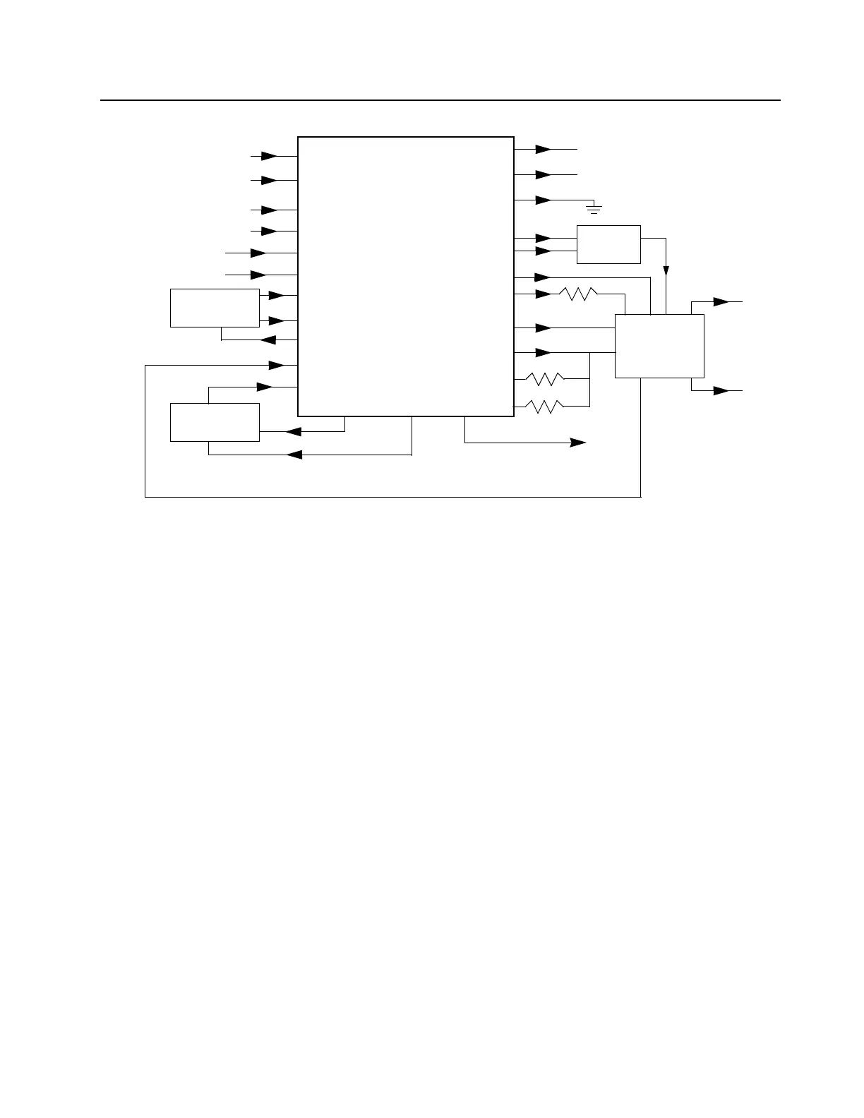
Figure 5-3 UHF Synthesizer Block Diagram
A voltage of 5V applied to the super filter input (U4201 pin 30) supplies an output voltage of 4.5
VDC(VSF) at pin 28. It supplies the VCO, VCO modulation bias circuit (via R4322) and the
synthesizer charge pump resistor network (R4251, R4252). The synthesizer supply voltage is
provided by the 5V regulator U4211.
In order to generate a high voltage to supply the phase detector (charge pump) output stage at
pin 47 VCP (U4201-47), a voltage of 13 VDC is being generated by the positive voltage multiplier
circuitry (D4201, C4202, C4203). This voltage multiplier is basically a diode capacitor network
driven by two (1.05MHz) 180 degrees out of phase signals (U4201-14 and -15).
Output LOCK (U4201-4) provides information about the lock status of the synthesizer loop. A high
level at this output indicates a stable loop. IC U4201 provides the 16.8 MHz reference frequency at
pin 19.
The serial interface (SRL) is connected to the µP via the data line DATA (U4201-7), clock line
CLK (U4201-8), and chip enable line CSX (U4201-9).
DATA
CLK
CEX
MODIN
VCC, DC5V
XTAL1
XTAL2
WARP
PREIN
VCP
REFERENCE
OSCILLATOR
VOLTAGE
MULTIPLIER
DATA (U0101 PIN 100)
CLOCK (U0101 PIN 1)
CSX (U0101 PIN 2)
MOD IN (U0221 PIN 40)
+5V (U4211 PIN 1)
7
8
9
10
13, 30
23
24
25
32
47
VMULT2 VMULT1
BIAS1
SFOUT
AUX3
AUX4
IADAPT
IOUT
GND
FREFOUT
LOCK
4
19
6, 22, 33, 44
43
45
3
2
28
14
15
40
FILTERED 5V
STEERING
LOCK (U0101 PIN 56)
PRESCALER IN
FREF (U0221 PIN 34)
39
BIAS2
41
48
5, 20, 34, 36
+5V (U4211 PIN 1)
AUX1
VDD, DC5V
MODOUT
U4201
LOW VOLTAGE
FRACTIONAL-N
SYNTHESIZER
AUX2
1 (NU)
BWSELECT
VCO Bias
TRB
To IF
Section
TX RF INJECTION
(1ST STAGE OF PA)
LO RF INJECTION
VOLTAGE
CONTROLLED
OSCILLATOR
LINE
2-POLE
LOOP
FILTER
 Loading...