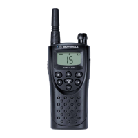
Troubleshooting Flow Chart for VCO Section 13: 3-5
6881091C63-F
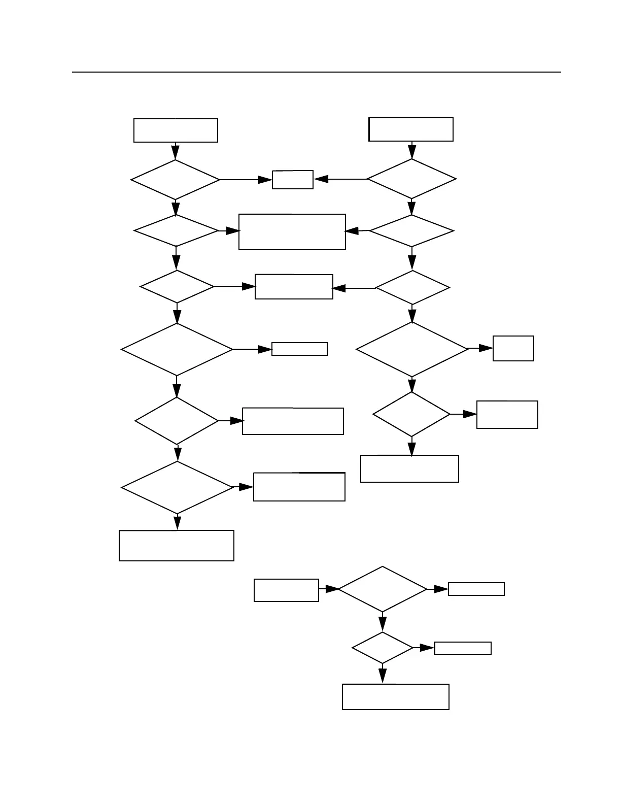
4.0 Troubleshooting Flow Chart for VCO
Are Q5332
Base at 0.7 V
Collector at 4.5 V
Emitter at 110 mV
Are Q5301
Base at 2.4 V
Collector at 4.5 V
Emitter at 1.7 V
Are Q5311
Base = 1.9 V
Collector = 4.5 V
Emitter = 1.3 V
Low or no RF Signal
at TP5003
Visual check
of board
OK?
35 mV DC at
U5301 Pin 19
NO
YES
Replace Q5301
at base of Q5332
NO
NO
NO
NO
YES
YES
YES
YES
Low or no RF Signal
at input to PA
4.8 VDC at
U5301 Pin 19
Is RF available
at U5401
YES
YES
YES
YES
NO
NO
NO
NO
NO
Audio =180 mVrms
at “-” S
ide of
4.5 VDC
at CR5321
If C5321 and R5321 are OK,
then replace CR5321
Replace C5322
Replace C5325
NO
NO
YES
YES
TX VCO
RX VCO
Correct
Problem
Visual check
of board
OK?
Check runner
between U5201 Pin 2
and U5301 Pin 19
Is RF available
If all parts from U5301 Pin 8
to Base of Q5332 are OK,
replace U5301
If all parts associated
with the pins are OK,
replace Q5332
If all parts from collector
of Q5332 to TP5003 are
OK, Replace U5301
Power OK but
no modulation
If all parts from U5301 Pin 10
U5401 Pin 16 are OK,
replace U5301
Replace
Q5311
YES
YES
Make sure Synthesizer is
working correctly and runner
between U5201 Pin 28 and
U5301 Pin 14 & 18 are OK
4.5 VDC
OK?
OK?
OK?
C5325
at U5301 Pin 14 & 18
4.5 VDC
OK?
at U5301 Pin 14 &18
NO
Pin 16
If R5361 and
L5361 are OK,
replace U5301
 Loading...