VHF (136–174 MHz) 25–45 W Bipolar Frequency Synthesis Section 8: 2-7
6881091C63-F
Output LOCK (U3201-4) provides information about the lock status of the synthesizer loop. A high
level at this output indicates a stable loop. IC U3201 provides the 16.8 MHz reference frequency at
pin 19.
The serial interface (SRL) is connected to the µP via the data line DATA (U3201-7), clock line
CLK (U3201-8), and chip enable line CSX (U3201-9).
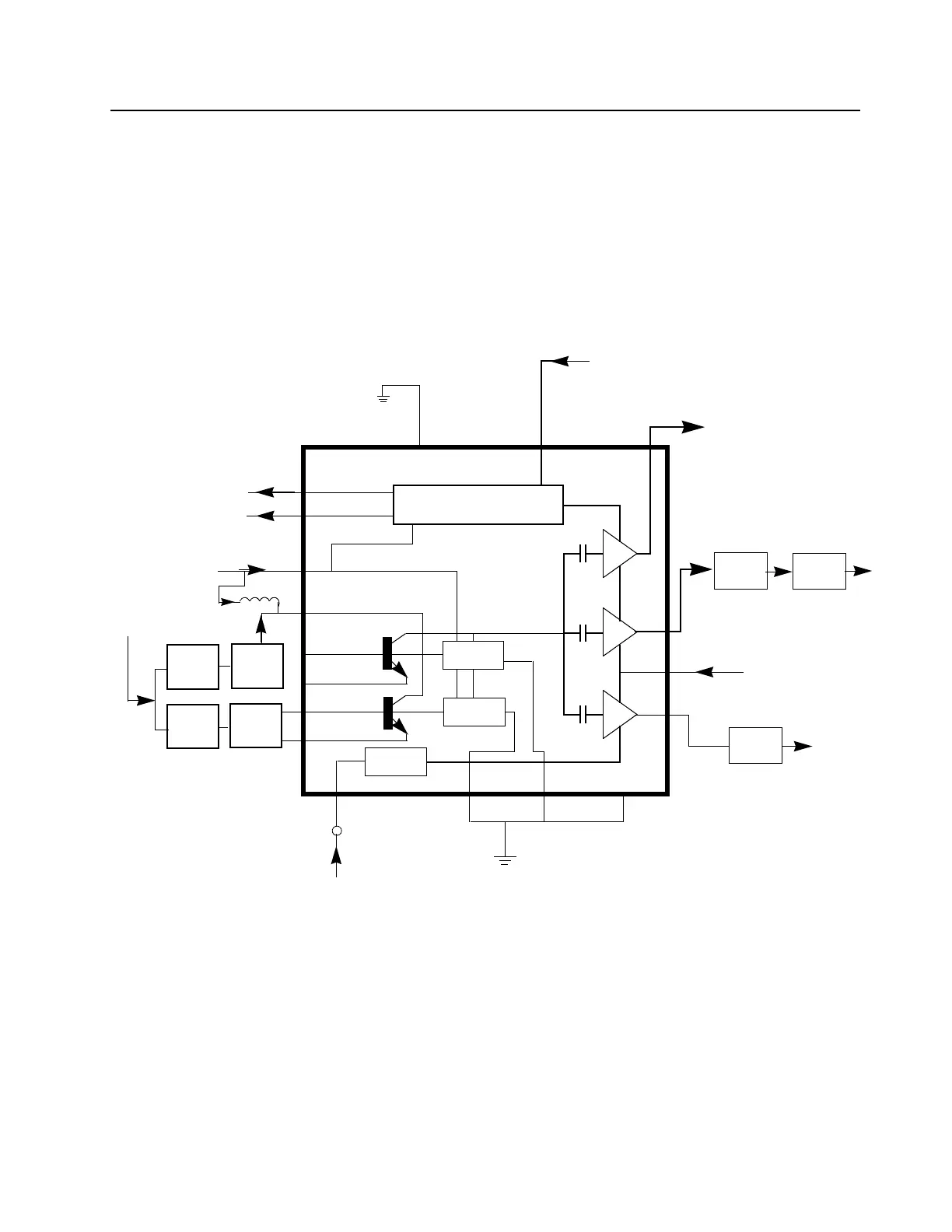
4.3 Voltage Controlled Oscillator (VCO)
The Voltage Controlled Oscillator (VCO) consists of the VCO/Buffer IC (VCOBIC, U3301), the TX
and RX tank circuits, the external RX buffer stages, and the modulation circuits.
Figure 8-4 VHF VCO Block Diagram
The VCOBIC together with the Fractional-N synthesizer (U3201) generates the required frequencies
in both the transmit and receive modes. The TRB line (U3301, pin 19) determines which tank circuits
and internal buffers are to be enabled. A high level on TRB enables the TX tank and TX output (pin
10), and a low enables the RX tank and RX output (pin 8). A sample of the signal from the enabled
RF output is routed from U3301, pin 12 (PRESC_OUT), via a low-pass filter, to U3201, pin 32
(PREIN).
Presc
RX
TX
Matching
Network
Low-Pass
Filter
Attenuator
Pin8
Pin14
Pin10
(U3211 Pin1)
VCC Buffers
TX RF Injection
U3201 Pin 32
AUX3 (U3201 Pin2)
Prescaler Out
Pin 12Pin 19
Pin 20
TX/RX/BS
Switching Network
U3301
VCOBIC
Rx
Active Bias
Tx
Active Bias
Pin2
Rx-I adjust
Pin1
Tx-I adjust
Pins 9,11,17
Pin18
Vsens
Circuit
Pin15
Pin16
RX VCO
Circuit
TX VCO
Circuit
RX Tank
TX Tank
Pin7
Vcc-Superfilter
Collector/RF in
Pin4
Pin5
Pin6
RX
TX
(U3201 Pin28)
Rx-SW
Tx-SW
Vcc-Logic
(U3211 Pin1)
Steer Line
Voltage
(VCTRL)
Pin13
Pin3
TRB IN
LO RF INJECTION
Q3304
Q3301
 Loading...