2-13
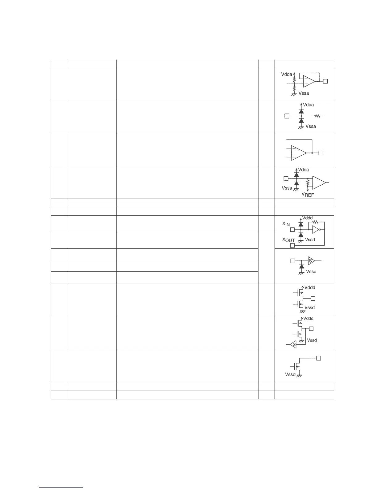
Pin Descriptions
Pin No. Pin Function I/O Pin circuit type
Reference voltage output (Vdda/2) Output1 VREF
Base band (multiplex) signal input Input2 MPXIN
Subcarrier output (filter output) Output5 FLOUT
Subcarrier input (comparator input) Input6 CIN
Analog system power supply (+5 V) — —3 Vdda
Analog system ground — —4 Vssa
Crystal element output (4.332 MHz) Output8 XOUT
RDS data output Output14 RDDA
RDS clock output (master mode)
RDS clock input (slave mode)
I/O15 RDCL
RDS ID/ready output (Active low) Output
—
—
—
—
16 RDS-ID/READY
Digital system power supply (+5 V)11 Vddd
Digital system ground10 Vssd
Test input7 TEST
Crystal element input (or external reference signal input)
Input
9 XIN
Readout mode setting (0: master, 1: slave)12 MODE
RDS ID and RAM reset (Active high logic)13 RST