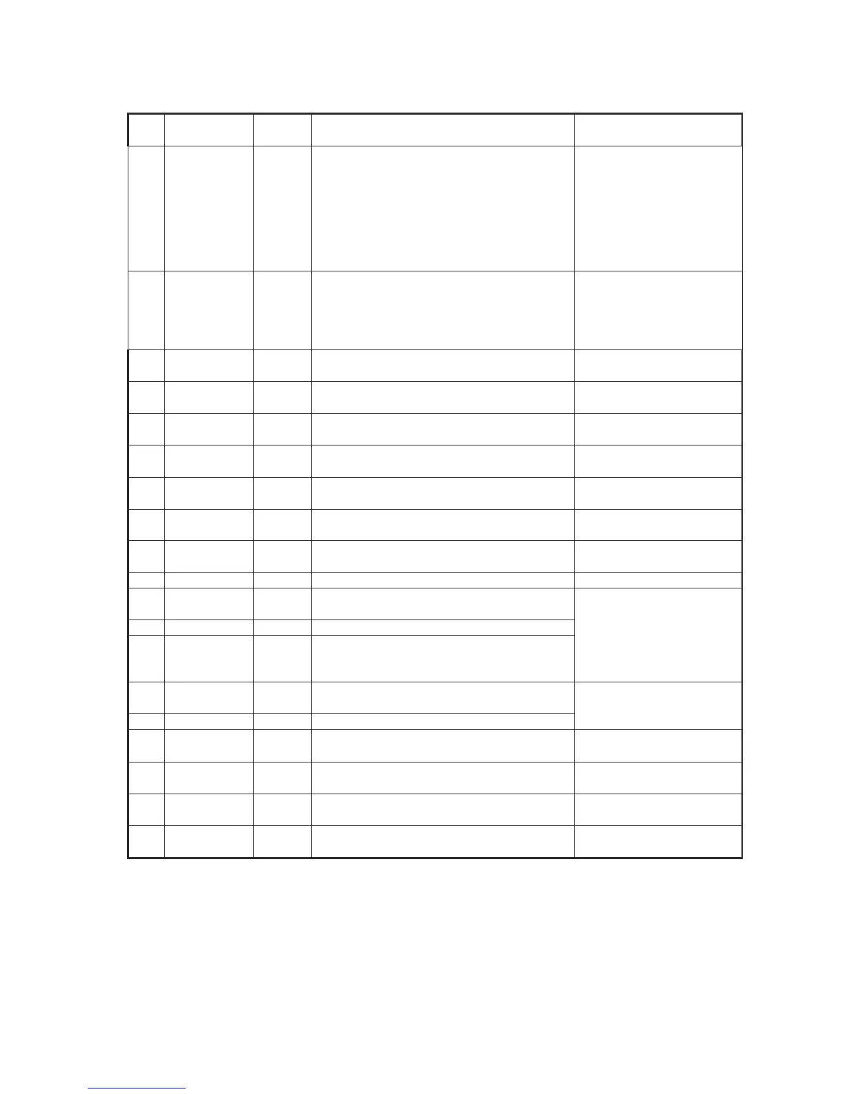
2-19
Pin
No.
Pin name I/O Description Remark
17
SFSY
(EMPH)
(LOCK)
(MONIT)
O
3I/F
Pin for outputting the playback frame sync
signal.
(Emphasis flag output pin.
ENPH on: "H". EMPH off: "L".
The output polarity can be switched, using a
command.)
(LOCK signal)
(Pin for monitoring signals in the DSP.)
7.35kHz
(At this pin, flags in the
DSP and PLL-circuit clock
can be monitored, using
microcontroller commands.
The pin also outputs text
data serially.)
18
ZDET
(DATA)
(COFS)
O
3I/F
Output pin for zero detection flag for the
1-bit DAC.
(Pin for outputting subcode P to W data)
(Error Correstion Frame Clock 7.35kHz
output)
Valid also for 1-bit DAC
external inputs.
19 GPIN
I/O
3I/F
General-purpose I/O㧔DSP㧕
General-purpose I/O
(input after a reset).
20 VSS1 —
1.5V grounding pin dedicated to the Digital
circuit.
—
21 VDD1 —
1.5 V supply voltage pin dedicated to the
Digital circuit.
—
22 XVSS3 —
Grounding pin for the system clock
oscillation circuit.
—
23 XI
I
3AI/F
Input pin for the system clock oscillation
circuit.
—
24 XO
O
3AI/F
Output pin for the system clock oscillation
circuit.
Input to the internal MCK.
25 XVDD3 —
3.3 V supply voltage pin for the system
clock oscillation circuit.
—
26 DVSS3 — Grounding pin for the 1-bit DAC. —
27 RO
O
3AI/F
Output pin for normal R-channel data for
the 1-bit DAC.
28 DVDD3 — 3.3 V supply voltage pin for the 1-bit DAC.
29 DVR O Reference voltage pin for the 1-bit DAC.
No capacitor is required at
the DVR pin unless the
built-in 1-bit DAC is used.
3.3 V must be applied
across the DVDD3 and
DVSS3 pins, however.
30 LO
O
3AI/F
Output pin for normal L-channel data for
the 1-bit DAC.
31 DVSS3
—
Grounding pin for the 1-bit DAC.
—
32 VSS3
—
3.3 V grounding pin dedicated to the I/F
circuit.
—
33 VDD3
—
3.3 V supply voltage pin dedicated to the I/F
circuit.
—
34 VDDM
—
1.5 V supply voltage pin dedicated to the
DSP/1Mbit SRAM circuit.
—
35 VSS1
—
1.5V grounding pin dedicated to the
DSP/1Mbit SRAM circuit.
—