Chapter 4 Digital I/O
E Series User Manual 4-4 ni.com
voltage across the pull-down resistor above a TTL-low level of 0.4 VDC.
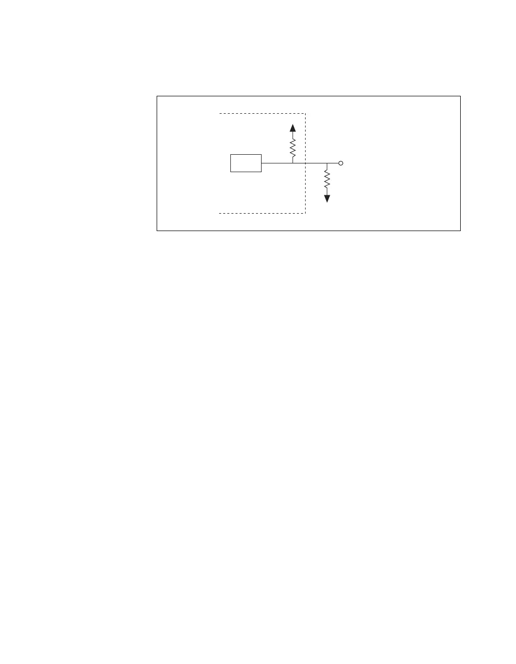
Figure 4-2 shows the DIO configuration for high DIO power-on state.
Figure 4-2. DIO Configuration for High DIO Power-On State
The following steps show how to calculate the value of R
L
needed to
achieve a TTL-low power-on state for a single DIO line.
Using the following formula, calculate the largest possible load to maintain
a logic low level of 0.4 V and supply the maximum driving current:
V = I × R
L
→ R
L
= V/I
where:
V = 0.4 V Voltage across R
L
I = 46 µA (4.6 V across the 100 kΩ pull-up resistor) + 10 µA (10 µA
maximum leakage current)
Therefore:
R
L
= 7.1 kΩ (0.4 V/56 µA)
This resistor value, 7.1 kΩ, provides a maximum of 0.4 V on the DIO line
at power-on. You can substitute smaller resistor values to lower the voltage
or to provide a margin for V
cc
variations and other factors.
Timing Specifications
(NI 6016 and NI 6025E Devices Only) This section lists the timing
specifications for handshaking with the P3.<0..7> lines. The handshaking
lines STB* and IBF synchronize input transfers. The handshaking lines
OBF* and ACK* synchronize output transfers. Table 4-2 describes signals
appearing in the handshaking diagrams.
Device
Digital I/O Line
82C55
100 k
GND
+5 V
R
L
 Loading...