Chapter 2 Theory of Operation
©
National Instruments Corporation 2-5 PCI E Series RLPM
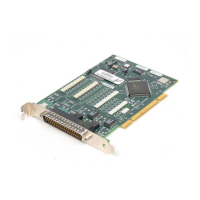
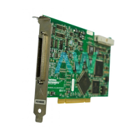
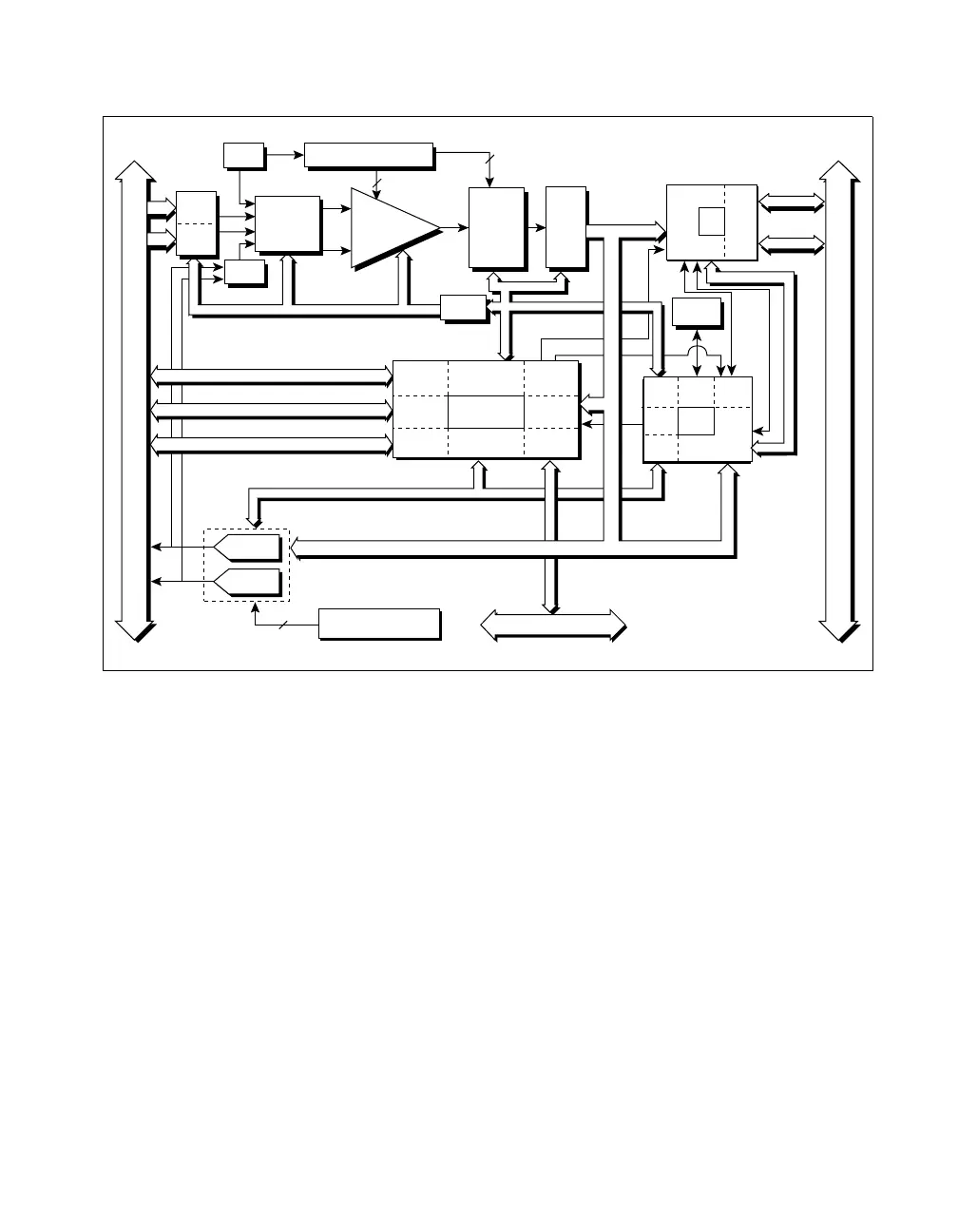
Figure 2-5. PCI-MIO-16XE-50 Block Diagram
The following major components make up the PCI E Series boards:
• PCI bus interface circuitry with Plug and Play capability (MITE)
• Analog input circuitry
• Analog trigger circuitry
• Analog output circuitry
• Digital I/O circuitry
• Timing I/O circuitry (DAQ-STC)
• RTSI bus interface circuitry
The internal data and control buses interconnect the components. Notice
that the DAQ-STC is the timing engine that provides precise timing signals
for the analog input and output operations. The timing I/O circuitry
information in this manual is skeletal in nature and is sufficient in most
cases. For register-level programming information, refer to the DAQ-STC
Technical Reference Manual.
Timing
PFI / Trigger
I/O Connector
2
2
RTSI Bus
PCI Bus
Digital I/O (8)
16-Bit
Sampling
A/D
Converter
Configuration
Memory
+
Programmable
Gain
Amplifier
–
Calibration
Mux
Mux Mode
Selection
Switches
Analog
Muxes
Voltage
REF
Calibration
DACs
4
Calibration
DACs
DAC0
DAC1
DAQ - STC
Analog Input
Timing/Control
Analog Output
Timing/Control
Digital I/O
Trigger
Counter/
Timing I/O
RTSI Bus
Interface
DMA/
Interrupt
Request
Bus
Interface
(8)
(8)
Data (16)
AI Control
Data (16)
AO Control
ADC
FIFO
EEPROM
Address/Data
Control
Analog
Input
Control
EEPROM
Control
DMA
Interface
MIO
Interface
DAQ-STC
Bus
Interface
Analog
Output
Control
I/O
Bus
Interface
MITE
Generic
Bus
Interface
PCI
Bus
Interface
IRQ
DMA
Address (5)
 Loading...