Chapter 3 Register Map and Descriptions
©
National Instruments Corporation 3-3 PCI E Series RLPM
Register Sizes
Two different transfer sizes for read-and-write operations are available on the
computer—byte (8-bit) and word (16-bit). Table 3-1 shows the size of each PCI E Series
register. For example, reading the ADC FIFO Data Register requires a 16-bit (word) read
operation at the selected address, whereas writing to the Misc Command Register requires
an 8-bit (byte) write operation at the selected address. For proper board operation you must
adhere to these register size accesses. Avoid performing a byte access on a word location or
performing a word access on a byte location; these are invalid operations. The register sizes
are very important.
Register Descriptions
This section discusses each of the PCI E Series registers in the order shown in Table 3-1. Each
register group is introduced, followed by a detailed bit description. The individual register
description gives the address, type, word size, and bit map of the register, followed by a
description of each bit.
The register bit map shows a diagram of the register with the MSB shown on the left (bit 15
for a 16-bit register, bit 7 for an 8-bit register), and the LSB shown on the right (bit 0). A
square represents each bit and contains the bit name. An asterisk (*) after the bit name
indicates that the bit is inverted (negative logic).
In many of the registers, several bits are labeled Reserved. When a register is read, these bits
may appear set or cleared but should be ignored because they have no significance. When you
write to a register, set these bits to zero.
Misc Register Group
The three registers making up the Misc Register Group include two command registers that
control the serial DACs, EEPROM, and analog trigger source, and one status register that
includes EEPROM information.
Bit descriptions of the three registers making up the Misc Register Group are given on the
following pages.
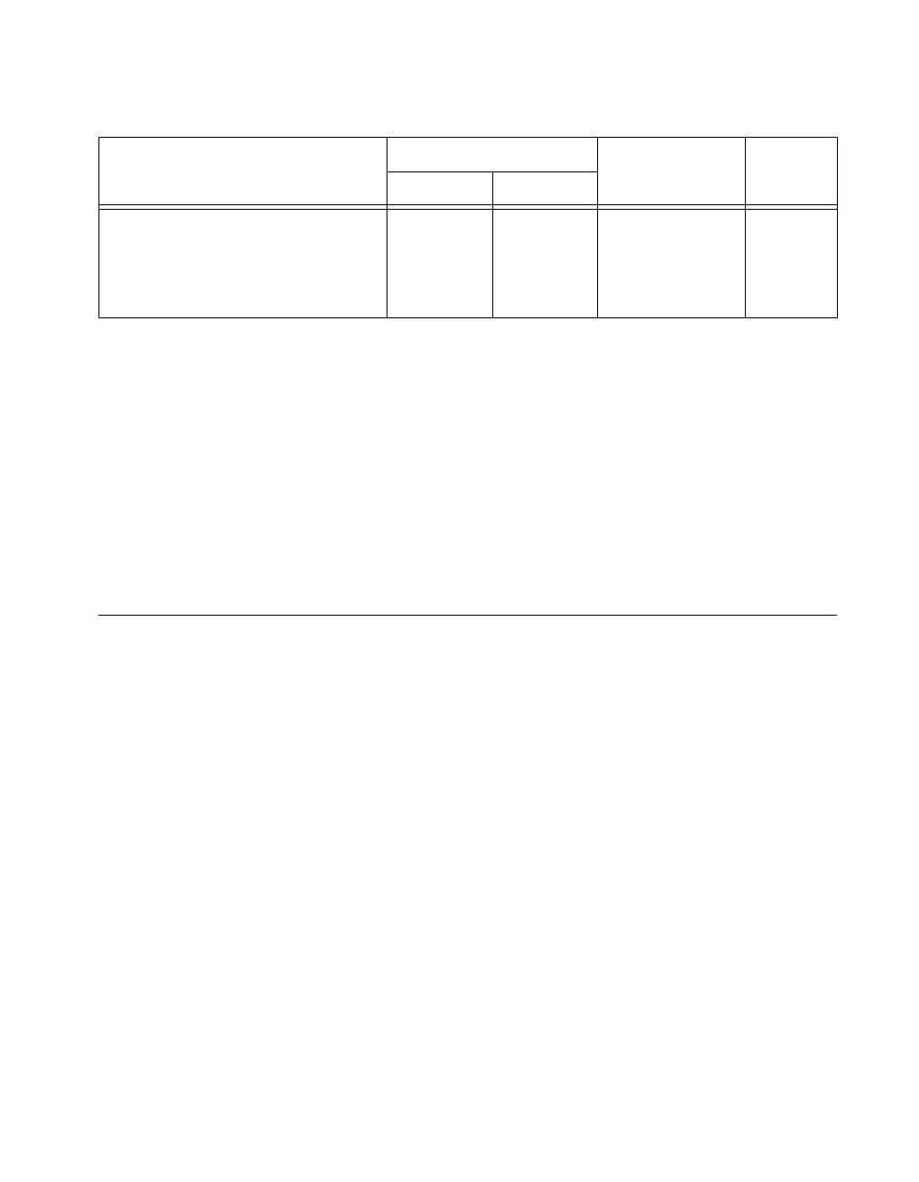
Table 3-2.
PCI E Series Windowed Register Map
Register Name
Offset Address
Type SizeHex Decimal
FIFO Strobe Register Group
Configuration Memory Clear
ADC FIFO Clear
DAC FIFO Clear
52
53
54
82
83
84
Write-only
Write-only
Write-only
16-bit
16-bit
16-bit
 Loading...