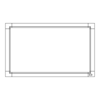
7. Horizontal drive and power supply output
Circuit Diagram
Description of the circuit:
1) R1, T1 and Q2 compose the horizontal driving circuit, and the transistor Q1 generates a horizontal
output through the driving signal.
IB1 = I
CPMAX
/ Q1h
feMIN
I
B2
¡Ü¡Ü
¡Ü¡Ü
¡Ü 3I
B1
di/dt
¡Ü¡Ü
¡Ü¡Ü
¡Ü 3.3 A/US
2) The resistor R2 corrects the current IB1, the resistor R3 works as a damping resistor and leak
resistor, and the diode D2 works as a discharging device and polar body.
As long as the transistor Q1 is OFF, the discharge is accelerated and the storage time (Tstg) is
shortened.
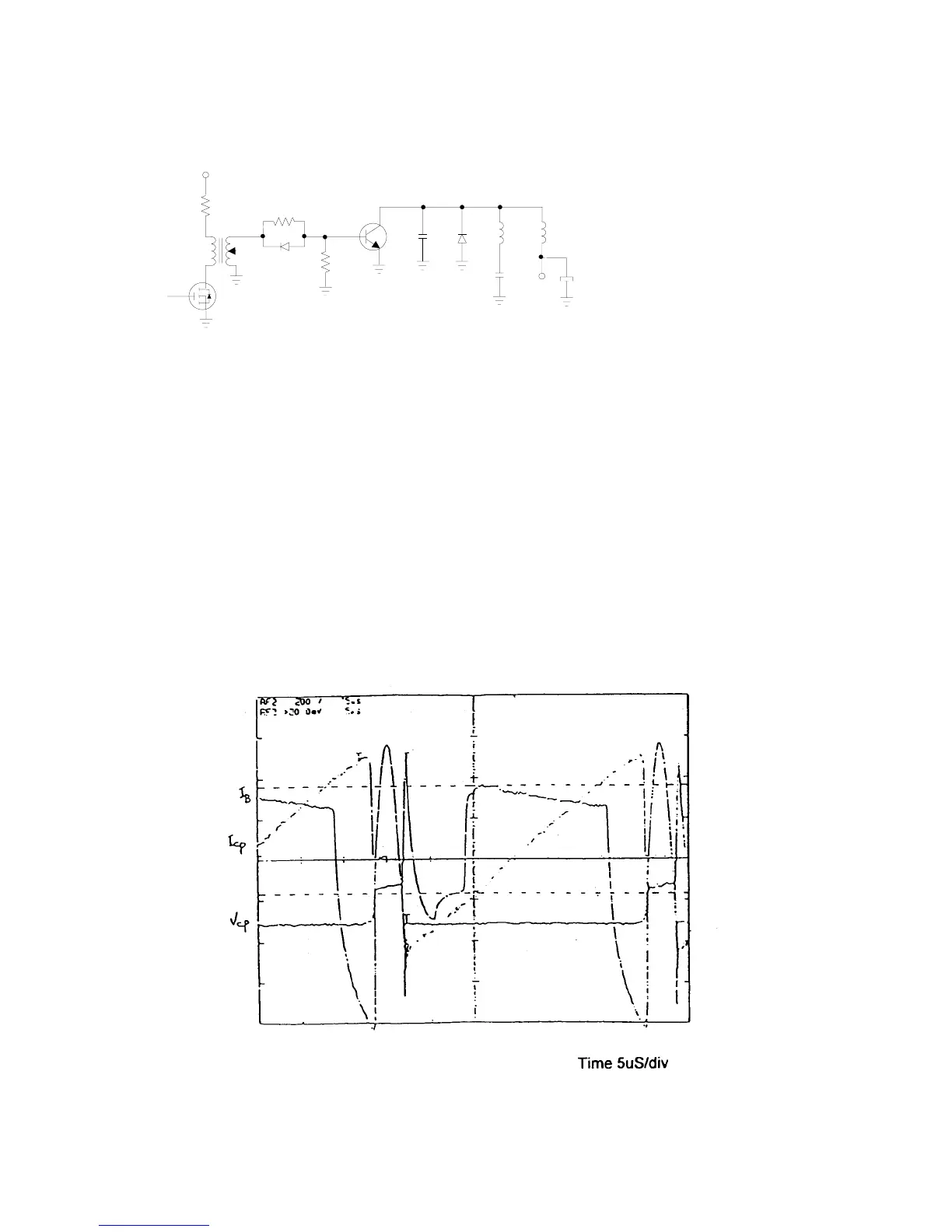
3)H-OUT circuit waveform
VCC
T1
R2
D2
R1
Q2
R3
Q1
CT
D1
DR
CS
B+
C2
+
63