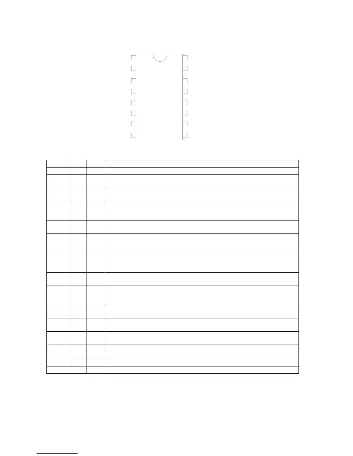
1.0 CONNECTION DIAGRAM
(16 PINS PDIP 300 MIL PACKAGE)
2.0 PIN DESCRIPTIONS
1
2
3
4
5
6
7
89
10
11
12
13
14
15
16
MTV016-N
VSSA
VCO
RP
VDDA
HFLB
SSB
SDA
SCK
VSS
ROUT
GOUT
BOUT
FBKG
HTONE
VFLB
VDD
Name I/O Pin# Function
VSSA - 1
Analog ground.
This ground pin is used to internal analog circuitry.
VCO I/O 2
Volta
e Control Oscillator.
This pin is used to control the internal oscillator
frequency by DC voltage input from external low pass filter.
RP I/O 3
Bias Resistor.
The bias resistor is used to regulate the appropriate bias
current for internal oscillator to resonate at specific dot frequency.
VDDA - 4
Analog power supply.
Positive 5 V DC supply for internal analog circuitry.
And a 0.1uF decouplin
capacitor should be connected across to VDDA and
VSSA.
HFLB I 5
Horizontal input.
This pin is used to input the horizontal synchronizing
signal. It has an internal 100 k
Ω
pull-up resistor.
SSB I 6
Serial interface enable.
It is used to enable the serial data interface and is
also used to select I²C or SPI bus operation. If this pin is left floatin
I²C bus
is enable. Otherwise the SPI bus is enabled.
SDA I 7
Serial data input.
The external data transfer through this pin to internal
display registers and control registers. It has an internal 100 k
Ω
pull-up
resistor.
SCK I 8
Serial clock input.
The clock input pin is used to synchronize the data
transfer. It has an internal 100 k
Ω
pull-up resistor.
VDD - 9
Digital power supply.
Positive 5 V DC supply for internal digital circuitry
and a 0.1uF decouplin
capacitor should be connected across to VDD and
VSS.
VFLB I 10
Vertical input.
This pin is used to input the vertical synchronizing signal. It
has an internal pull-up resistor.
HTONE O 11
Half tone out
ut.
This pin is used to attenuate the external R
B amplifiers
gain for the transparent windowing effect.
FBKG O 12
Fast Blankin
ut.
It is used to cut off the external R
nals while
this chip is displaying characters or windows.
BOUT O 13
Blue color output.
It is a blue color video signal output.
GOUT O 14
Green color output.
It is a green color video signal output.
ROUT O 15
Red color output.
It is a red color video signal output.
VSS - 16
Digital ground.
This ground pin of internal digital circuitry.
73