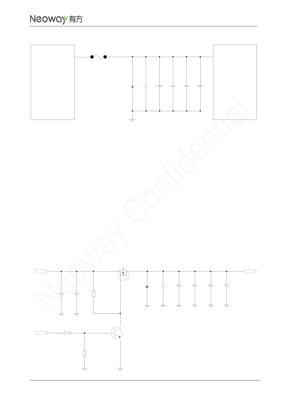
⚫
The maximum input voltage for the module is 4.3 V and the typical value is 3.9 V.
⚫
SMF5.0AG (Vrwm=5V&Pppm=200W) is recommended at D1. The protection voltage across D1
should not exceed the maximum input voltage the module can bear.
Place TVS close to the input interface of the power supply to clamp the surge voltage before it
enters back-end circuits. Therefore, the back-end components and the module are protected.
⚫
A large bypass tantalum capacitor (220 μF or 100 μF) or aluminum capacitor (470 μF or 1000
μF) is expected at C1 to reduce voltage drops during bursts. Its maximum safe operating voltage
should be larger than 1.5 times the voltage across the power supply.
⚫
Place low-ESR bypass capacitors close to the module to filter out high-frequency noise from the
power supply.
A controllable power supply is preferable if the module is used in harsh conditions. Figure 3-2 shows
the recommended schematic design.
Figure 3-2 Recommended design 2