Schematic Design Guidelines
⚫
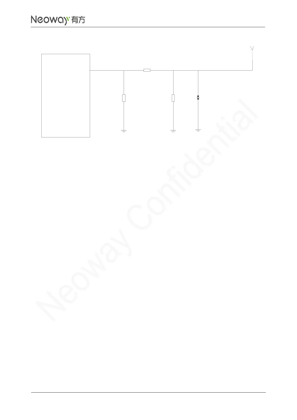
Element components in the above figures are capacitors, inductors, and 0 Ω resistors. Place
these RLC components as close to the antenna interface as possible.
⚫
Add an ESD protector. The protector can be a TVS diode with a junction capacitance of lower
than 0.5 pF. Ensure that the reverse breakdown voltage of the TVS is greater than 10 V (above
15V is recommended).
PCB Layout Guidelines
⚫
Lay copper foil around RF connector. Dig as many via holes as possible on the copper to ensure
lowest grounding impedance.
⚫
The traces between N11 and the antenna connector should be as short as possible. Control the
trace impedance to 50 Ω.
⚫
If customers adopt SMA connector, big RF solder pad might result in great parasitic capacitance,
which will affect the antenna performance. Remove the copper on the first and second layers
under the RF solder pad and keep complete reference ground plane on the third layer.
⚫
Keep clearance (no ground) area at least on the layer the antenna solder pad resides and
ensure that the neighboring reference ground is connected to the main ground properly.