⚫
Place low-ESR bypass capacitors close to the module to filter out high-frequency noise from the
power supply.
The following design is recommended for 5.5 V to 24 V input.
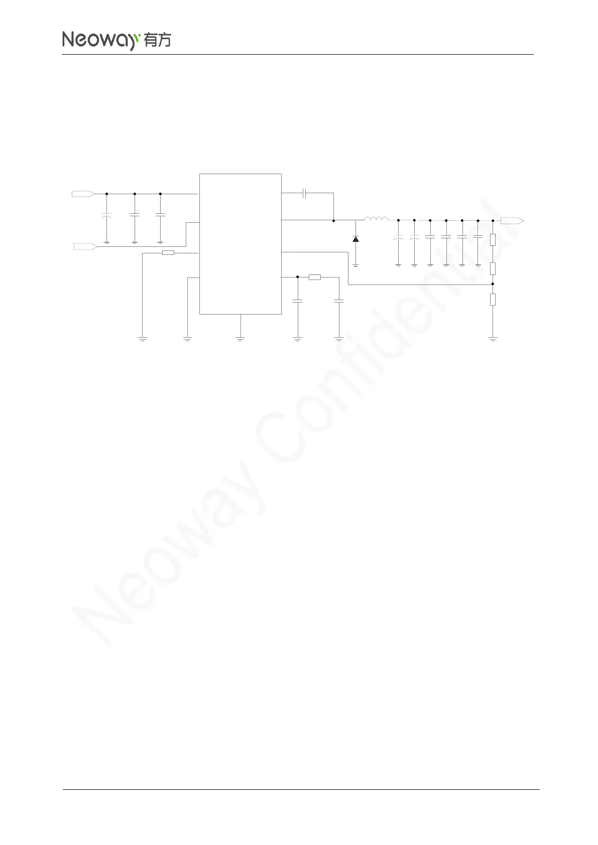
Figure 3-4 Recommended design 4
⚫
Select DC-DC that outputs a maximum current larger than 2 A when the output of power supply
is much larger than the permissible voltage across VBAT.
⚫
500 kHz or higher switching frequency is recommended for DC-DC.
⚫
The switching frequency of DC-DC might produce EMC noise and it determines the performance
of end products.
⚫
Add surge protection to the front end of the power supply circuit if automotive battery supplies
power. The maximum safe operating voltage of the component should be larger than 42 V.
⚫
Place TVS2 close to the input interface of the power supply to clamp the surge voltage before it
enters back-end circuits. Therefore, the back-end components and the module are protected.
⚫
Place C7 close to the module. A large bypass tantalum capacitor (220 μF or 100 μF) or
aluminum capacitor (470 μF or 1000 μF) is expected to reduce voltage drops during bursts. Its
maximum safe operating voltage should be larger than 1.5 times the voltage across the power
supply.
⚫
Place low-ESR bypass capacitors close to the module to filter out high-frequency noise from the
power supply.
PCB Layout Guidelines
⚫
TVS diodes dissipate the transient pulse power during a surge and have a short response time.
Place the TVS as close to the interface as possible to ensure that the surge voltage can be
clamped before the pulse is coupled to the neighbor traces.
⚫
Place filer capacitors close to the power pin of the module to filter out the high-frequency noise
from the power supply.