⚫
If the UART does not match the logic voltage of the MCU, add an external level shifting circuit.
Three types of level shifting circuit are recommended based on the logic level quality. The first one is
preferred and the other two are cost-effective simple circuits. Note their application senarios.
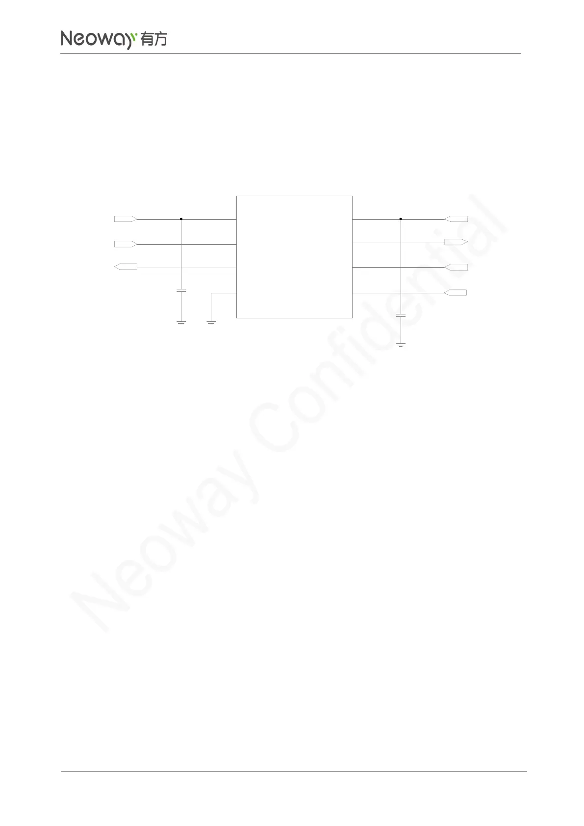
Level shift chip is recommended if the level of MCU is higher than 3.3 V or the baudrate is higher
than 1 MHz. Figure 3-10 shows the reference design.
Figure 3-10 Level shifting circuit 1
NLSX4373 is a dual-supply level shifter, the rate of which is up to 20 Mb/s.
⚫
VL is the reference voltage of IO_VL1 and IO_VL2, ranging from 1.5 V to 5.5 V.
⚫
VCC is the reference voltage of IO_VCC1 and IO_VCC2, ranging from 1.5 V to 5.5 V.
⚫
EN is the enable pin, which works at a voltage of greater than VL-0.2V.
In the above circuit, the EN pin is connected to VDD_1P8 and the level shifter is always working.
If the low level at MCU_UART (V
IL
) is lower than 200 mV, use level shifting circuit in Figure 3-11.