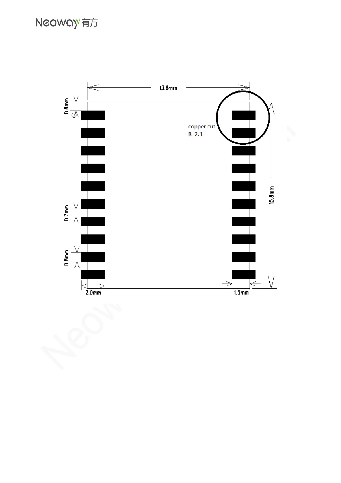
7.2 Application Foot Print
Figure 7-2 Recommended PCB foot print (Unit: mm)
7.3 Stencil
The recommended stencil thickness is at least 0.12 mm to 0.15 mm.
7.4 Solder Paste
Do not use the kind of solder paste different from our module technique.
⚫
The melting temperature of solder paste with lead is 35 °C lower than that of solder paste
without lead. It is easy to cause voiding for LCC inside the module after second reflow soldering.