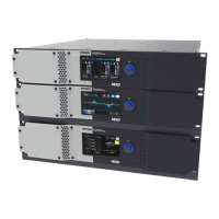
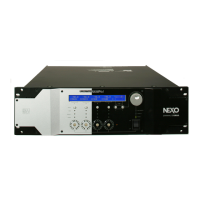
NXAMP4x1
26
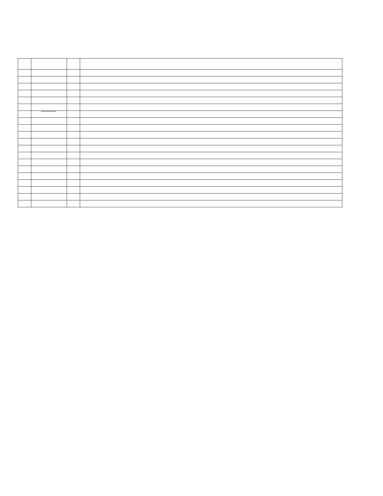
■ LSI PIN DESCRIPTION
1
2
3
4
5
6
7
8
9
10
11
12
13
14
15
16
17
18
19
20
VINL
V
INR
V
REF1
V
REF2
VCC
AGND
PDWN
BYPAS
TEST
LRCK
BCK
DOUT
DGND
V
DD
SCKI
OSR
FMT0
FMT1
MODE0
MODE1
Analog input, L-channel
Analog input, R-channel
Reference voltage 1 decoupling capacitor
Reference voltage 2 decoupling capacitor
Analog power supply, 5 V
Analog GND
Power-down control, active-low
(2)
HPF bypass control / LOW: Normal mode (dc reject); HIGH: Bypass mode (through)
(2)
Test, must be connected to DGND
(2)
Audio data latch enable input/output
(1)
Audio data bit clock input/output
(1)
Audio data digital output
Digital GND
Digital power supply, 3.3 V
System clock input: 256 fs, 384 fs, 512 fs or 768 fs
(3)
Oversampling ratio select input / LOW: x 64 fs, HIGH: x 128 fs
(2)
Audio data format select input 0 / See data format section
(2)
Audio data format select input 1 / See data format section
(2)
Mode select input 0 / See data format section
(2)
Mode select input 1 / See data format section
(2)
PIN
NO.
NAME
I/O FUNCTION
• PCM1803ADBR (X7357B0) A/D CONVERTER CONTROL: IC035, IC036, IC037, IC038
I
I
–
–
–
–
I
I
I
I/O
I/O
O
–
–
I
I
I
I
I
I
(1) Schmitt trigger input
(2) Schmitt trigger input with internal pulldown (50 kΩ , typically), 5 V tolerant
(3) Schmitt trigger input, 5 V tolerant
 Loading...