Hardware description
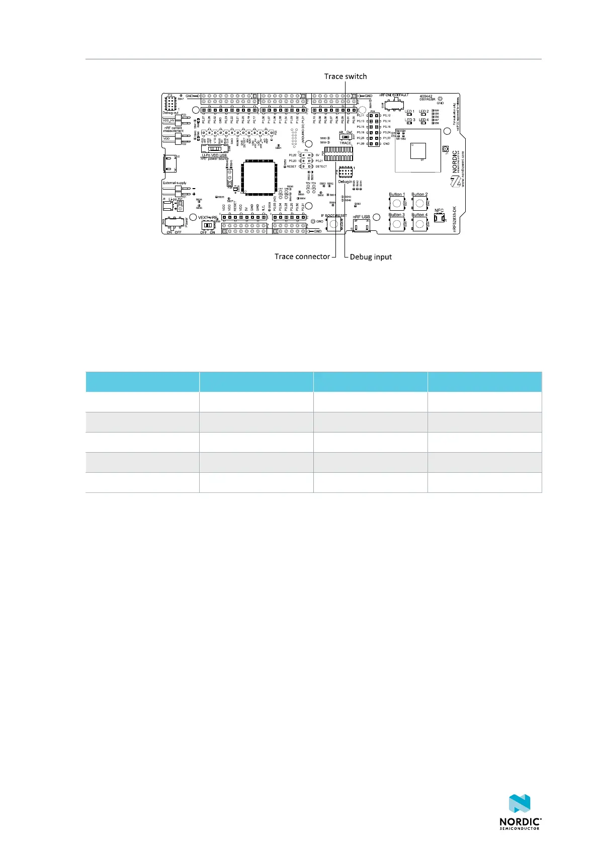
Figure 25: Debug input and trace connectors
For trace, a footprint for a 20-pin connector is available (P25). If trace functionality is required, it is
possible to mount a 2×10-pin 1.27-mm-pitch surface-mount pin header.
Some of the trace pins are by default used for other functionality on the DK. By sliding the TRACE switch
(SW7) from Def. to Alt., the functionality is moved to other GPIOs. See the following table:
GPIO Trace Default use Optional GPIO
P0.07 TRACECLK UART CTS P0.04
P1.00 TRACEDATA[0]
P0.11 TRACEDATA[1] Button 1 P1.07
P0.12 TRACEDATA[2] Button 2 P1.08
P1.09 TRACEDATA[3]
Table 5: Default and Trace GPIOs
The reference voltage for the debug input and trace is by default connected to VDD_nRF'. This can be
connected to the VDD by cutting SB60 and soldering SB59.
8.9 Debug output
The nRF52833 DK supports programming and debugging external boards with nRF51 or nRF52 SoCs. To
debug an external board with SEGGER J-Link OB IF, connect to the Debug out connector (P19) with a 10-
pin cable.
4452_198 v1.0.1
32
 Loading...