Power Supply
MPC5746R Hardware Design Guide, Rev. 1
NXP Semiconductors 3
low-voltage conditions. The monitoring capability is also used to ensure supply voltages and internal
voltages are within the required ranges before the microcontroller can exit reset. The MPC5746R MCU
supports three different input voltages:
• 1.25 V (required) for the internal logic. This supply may be provided externally or generated from
either the 3.3 V or 5.0 V supply using an external NPN Bipolar Junction Transistor (BJT) ballast
transistor and the internal 1.25 V regulator control.
• 5 V (required) for the Power Management controller, I/O, Debug, ADCs and external
communication interfaces
• 3.3 V (optional) for I/O, Debug and external communication interfaces
The 3.3 V supply required for the flash memory is generated by an on-chip regulator. This regulator
requires an external decoupling capacitor on VDD_HV_FLA.
3.1 Power Supply Signals and Pins
Table 3 lists all power domains with corresponding pin names.
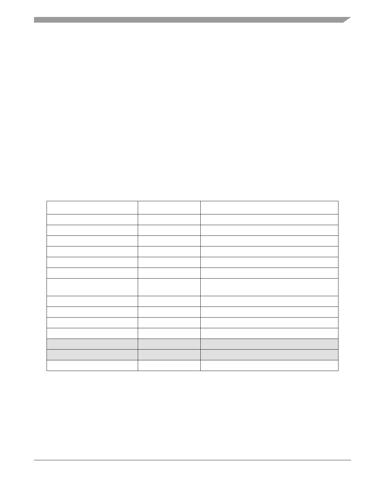
Table 3. MCU Supply Pins
Domain Name Supply Voltage
1
1
Nominal voltage, see MPC5746R Data Sheet for actual voltage specifications.
Description
VDD_LV
2
2
This supply may be optionally provided by the on-chip regulator using a pass transistor. See Section 3.1.2
1.25 V Core Logic Low Voltage Supply
VDD_HV_IO_MAIN 5.0 V Main I/O Voltage Supply
VDD_HV_ADV_SAR 5.0 V SAR ADC Voltage Supply
VDD_HV_ADR_SAR 5.0 V SAR ADC Voltage Reference
VDD_HV_ADV_SD 5.0 V Sigma-Delta ADC Voltage Supply
VDD_HV_ADR_SD 5.0 V Sigma-Delta ADC Voltage Reference
VDD_HV_IO_JTAG 3.3 V or 5.0 V
Production Device JTAG I/O and External Oscillator
Voltage Supply
VDD_HV_IO_FEC 3.3 V or 5.0 V Ethernet I/O Supply
VDD_HV_IO_MSC 3.3 V or 5.0 V Microsecond Channel I/O Supply
VDD_HV_PMC 5.0 V Power Management Controller Supply
VDD_HV_FLA
3
3
No connection to external supply required, but it does require a bypass capacitor.
3.3 V PMC Flash Regulator Bypass Capacitor
VDD_LV_BD
4
4
Only present on the 292 MAPBGA emulation device.
1.25 V Emulation Device Core Logic Low Voltage Supply
VDD_HV_IO_BD
4
3.3 V or 5.0 V Emulation Device Main I/O Voltage Supply
VDDSTBY
5
5
Ramp rate must be less than 16.6 kV/s as per limitation for the 0N94H mask set. Refer to the latest MPC5746R Data
Sheet for additional requirements.
1.3 V–5.9 V Standby RAM Supply Input

 Loading...


