Power Supply
MPC5746R Hardware Design Guide, Rev. 1
NXP Semiconductors 5
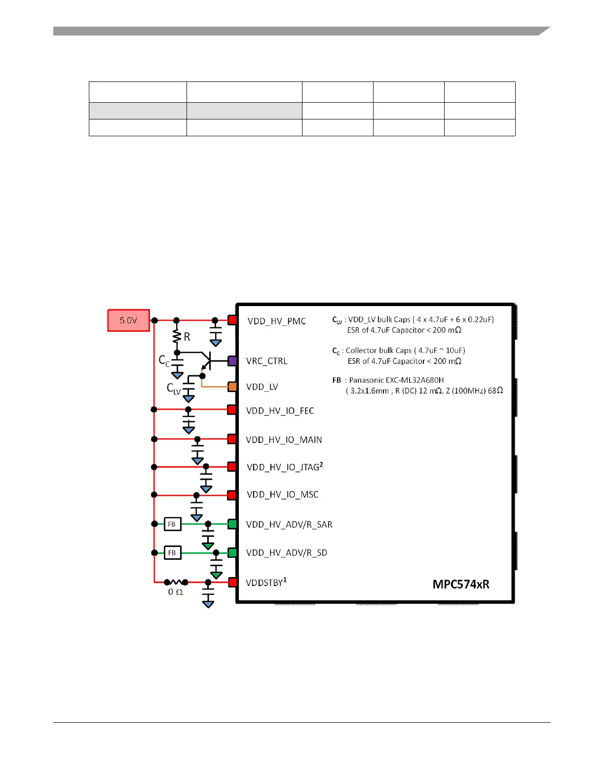
3.1.2 Single 5 V Supply
This topology uses a single 5 V supply for all I/O, with the internal regulator providing the 1.25 V for the
VDD_LV core supply. Note that most Fast Ethernet Controller (FEC) physical layer interfaces require 3.3
V signals, so the FEC would not normally be operational in this configuration.
Figure 1. Single 5 V Supply (no Ethernet)
1
VDDSTBY may need to be powered by a separate supply in the case where the standby SRAM data retention feature is required. This figure is intended to illustrate that a single 5 V supply
may be used where appropriate for the design.
2
VDD_HV_IO_JTAG is typically powered by a 3.3 V supply for compatibility with many debug tools. However if tools support 5 V or JTAG access is not required, a 5 V supply may be used and
the JTAG pins can be used as normal GPIO.
VDD_HV_IO_BD
4
3.3 V or 5.0 V - - -
VDDSTBY
4
1.3 V - 5.9 V 1 1 1
1
This supply may be optionally provided by the on-chip regulator using a pass transistor. See Section 3.1.2
2
Except bypass capacitor no connection to external supply required.
3
Only present on the 292 MAPBGA emulation device.
4
Ramp rate must be less than 16.6 kV/s as per limitation for the 0N94H mask set. Refer to the latest
MPC5746R Data Sheet for additional requirements.
Table 5. Number of power supply balls/pins versus package
Supply Domain Nominal Voltage 144LQFP 176LQFP 252BGA

 Loading...


