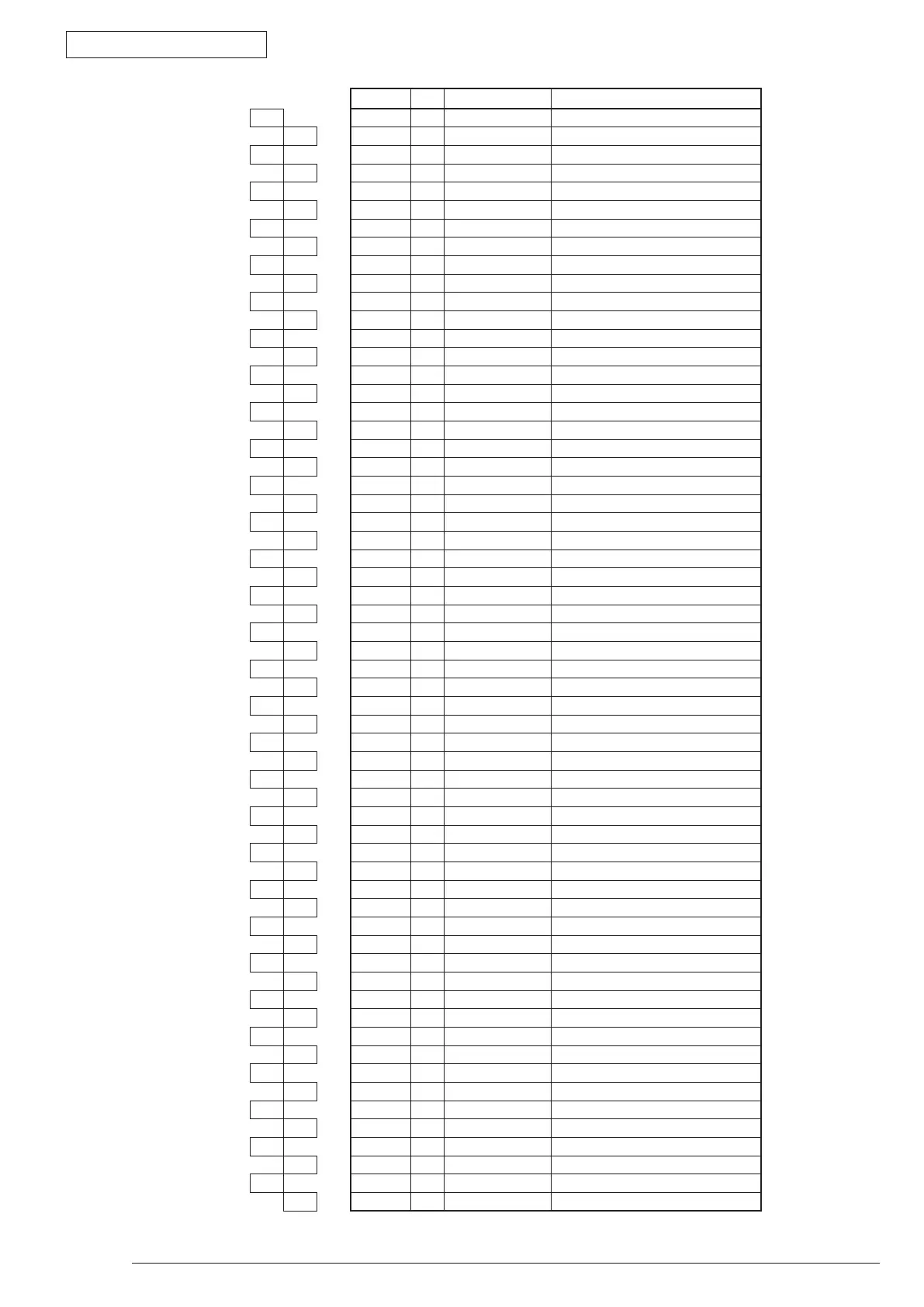
7.
Connection Diagram
43984801TH Rev.1
127 /
Oki Data CONFIDENTIAL
Pin No. I/O Signal Function
57 57 O VDD Logic Power
58 58 O VDD Logic Power
59 59 - NC Not Connected
60 60 - NC Not Connected
61 61 - NC Not Connected
62 62 - NC Not Connected
63 63 C VSS Logic Ground
64 64 C VSS Logic Ground
65 65 - NC Not Connected
66 66 - NC Not Connected
67 67 - NC Not Connected
68 68 - NC Not Connected
69 69 O VDD Logic Power
70 70 O VDD Logic Power
71 71 - NC Not Connected
72 72 - NC Not Connected
73 73 - NC Not Connected
74 74 - NC Not Connected
75 75 C VSS Logic Ground
76 76 C VSS Logic Ground
77 77 - NC Not Connected
78 78 - NC Not Connected
79 79 - NC Not Connected
80 80 - NC Not Connected
81 81 O VDD Logic Power
82 82 O VDD Logic Power
83 83 - NC Not Connected
84 84 - NC Not Connected
85 85 - NC Not Connected
86 86 - NC Not Connected
87 87 C VSS Logic Ground
88 88 C VSS Logic Ground
89 89 - NC Not Connected
90 90 C VSS Logic Ground
91 91 - NC Not Connected
92 92 O VDD Logic Power
93 93 O VDD Logic Power
94 94 O VDD Logic Power
95 95 O CKE1 Clock Enable 1
96 96 O CKE0 Clock Enable 0
97 97 - NC Not Connected
98 98 - NC Not Connected
99 99 O A12 Address Bus 12
100 100 O A11 Address Bus 11
101 101 O A9 Address Bus 9
102 102 O A8 Address Bus 8
103 103 C VSS Logic Ground
104 104 C VSS Logic Ground
105 105 O A7 Address Bus 7
106 106 O A6 Address Bus 6
107 107 O A5 Address Bus 5
108 108 O A4 Address Bus 4
109 109 O A3 Address Bus 3
110 110 O A2 Address Bus 2
111 111 O A1 Address Bus 1
112 112 O A0 Address Bus 0
113 113 O VDD Logic Power
114 114 O VDD Logic Power
115 115 O A10 Address Bus 10
116 116 O BA1 Bank Select 1