7.
Connection Diagram
43984801TH Rev.1
128 /
Oki Data CONFIDENTIAL
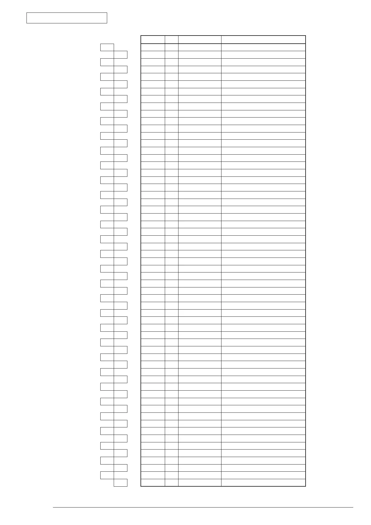
Pin No. I/O Signal Function
117 117 O BA0 Bank Select 0
118 118 O RAS Low Address Strobe
119 119 O WE Write Enable
120 120 O CAS Column-Address Strobe
121 121 O CS0N Chip Select 0
122 122 O CS1N Chip Select 1
123 123 O A13 Address Bus 13
124 124 - NC Not Connected
125 125 C VSS Logic Ground
126 126 C VSS Logic Ground
127 127 - NC Not Connected
128 128 - NC Not Connected
129 129 - NC Not Connected
130 130 - NC Not Connected
131 131 O VDD Logic Power
132 132 O VDD Logic Power
133 133 - NC Not Connected
134 134 - NC Not Connected
135 135 - NC Not Connected
136 136 - NC Not Connected
137 137 C VSS Logic Ground
138 138 C VSS Logic Ground
139 139 - NC Not Connected
140 140 - NC Not Connected
141 141 - NC Not Connected
142 142 - NC Not Connected
143 143 O VDD Logic Power
144 144 O VDD Logic Power
145 145 - NC Not Connected
146 146 - NC Not Connected
147 147 - NC Not Connected
148 148 - NC Not Connected
149 149 C VSS Logic Ground
150 150 C VSS Logic Ground
151 151 - NC Not Connected
152 152 - NC Not Connected
153 153 - NC Not Connected
154 154 - NC Not Connected
155 155 O VDD Logic Power
156 156 O VDD Logic Power
157 157 O VDD Logic Power
158 158 O CK1N Clock 1
159 159 C VSS Logic Ground
160 160 O CK1 Clock 1
161 161 C VSS Logic Ground
162 162 C VSS Logic Ground
163 163 - NC Not Connected
164 164 - NC Not Connected
165 165 - NC Not Connected
166 166 - NC Not Connected
167 167 O VDD Logic Power
168 168 O VDD Logic Power
169 169 O DQS6 Data Strobe 6
170 170 O DM6 Data Mask 6
171 171 - NC Not Connected
172 172 - NC Not Connected
173 173 C VSS Logic Ground
174 174 C VSS Logic Ground
175 175 - NC Not Connected
176 176 - NC Not Connected