Pin # Pin Name I/O Descri
tion Use
1 HSYNC I Horizontal S
nal Video and Audio
2VSYNC IVertical S
nal Video and Audio
3CGND Di
ital core GND. Ground
4 CVCC18 Di
ital core VCC. Connect to 1.8V su
. Power
5 SPDIF I S/PDIF Audio in
ut Video and Audio
6 MCLK I Audio In
ut Master Clock Video and Audio
7 SD3 I I2S Serial Data Video and Audio
8 SD2 I I2S Serial Data Video and Audio
9 SD1 I I2S Serial Data Video and Audio
10 SD0 I I2S Serial Data Video and Audio
11 WS I I2S Word Select Video and Audio
12 SCK I I2S Serial Clock Video and Audio
13 IOVCC IO Pin VCC. Connect to 3.3V su
. Power
14 IOGND IO Pin GND. Ground
15 CGND Di
ital core GND. Ground
16 CVCC18 Di
ital core VCC. Connect to 1.8V su
19 DSDA I/O DDC data Control
20 DSCL I/O DDC Clock Control
21 RSVDL I Reserved for use b
e, and must be tied LOW. Confirration/Pro
22 PGND1 TMDS Core PLL Ground. Ground
23 PVCC1 TMDS Core PLL Power. Connect to 3.3V su
GND. Ground
26 TXC- O
27 TXC+ O
28 AVCC Analo
. Power
29 TX0- O
30 TX0+ O
31 AGND Analo
GND. Ground
32 TX1- O
33 TX1+ O
34 AVCC Analo
. Power
35 TX2- O
36 TX2+ O
37 AGND Analo
GND. Ground
38 PVCC2 Filter PLL Power. Connect to 3.3V su
.POwer
39 PGND2 Filter PLL Ground. Ground
40 NC Not connected.
41 CI2CA I I2C device address select Control
42 RESET I Reset Pin. Active LOW Control
43 CSCL I I2C Clock Control
44 CSDA I/O I2C Data Control
45 CVCC18 Di
ital core VCC. Connect to 1.8V su
ital core GND. Ground
47 IOGND IO Pin GND. Ground
48 IOVCC IO Pin VCC. Connect to 3.3V su
. Power
49 D23 I
50 D22 I
51 D21 I
52 D20 I
53 D19 I
54 D18 I
55 D17 I
56 D16 I
57 D15 I
58 D14 I
59 CVCC18 Di
ital core VCC. Connect to 1.8V su
ital core GND. Ground
61 D13 I
62 D12 I
63 D11 I
64 D10 I
65 D9 I
66 IDCK I In
ut Data Clock Video and Audio
67 D8 I
68 D7 I
69 D6 I
70 D5 I
71 IOVCC IO Pin VCC. Connect to 3.3V su
. Power
72 IOGND IO Pin GND. Ground
73 CGND Di
ital core GND. Ground
74 CVCC18 Di
ital core VCC. Connect to 1.8V su
. Power
75 D4 I
76 D3 I
77 D2 I
78 D1 I
79 D0 I
80 DE I Data enable Video and Audio
Video and Audio
Video and Audio
Video and Audio
Video and Audio
12-bit Input Pixel Data Bus. These pins are used in 24-bit mode, single-
edge mode.
12-bit Input Pixel Data Bus. These pins are used in 24-bit mode, single-
edge mode.
12-bit Input Pixel Data Bus. These pins are used in 24-bit mode, single-
edge mode.
12-bit Input Pixel Data Bus. These pins are used in 24-bit mode, single-
edge mode.
24 EXT_SWING I
Voltage Swing Adjustment. The resistor between AVCC and this pin
determines the am
.
Differential signal data
TMDS output clock.
TMDS output data.
TMDS output data.
TMDS output data.
Differential signal data
Differential signal data
Differential signal data
Differential si
gnal data
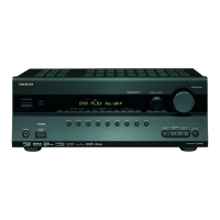
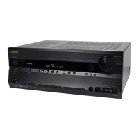
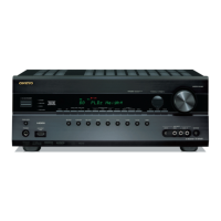
TX-SR604/604E/8460
IC BLOCK DIAGRAMS AND TERMINAL DESCRIPTIONS -31
Q8401 : SiI9030CTU (HDMI Transmitter)
TERMINAL DESCRIPTION