Do you have a question about the Onkyo TX-SR603E and is the answer not in the manual?
Provides specifications for the amplifier circuitry.
Outlines specifications for the FM and AM tuner.
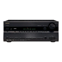
Covers general specifications like power supply and dimensions.
Details the process for replacing fuses, emphasizing safety.
Explains how to reset the unit to factory settings.
Describes how to check the microprocessor version.
Explains the battery-less memory backup system.
Covers the DC voltage detection for speaker protection checks.
Covers the current detection for speaker protection checks.
Focuses on power supply control and sensor checks.
Explains how to enter and use DSP debug mode.
Details the schematic for the audio input section.
Details the schematic for the DSP section.
Details the schematic for the first part of the power amplifier.
Details the schematic for the second part of the power amplifier.
Details the schematic for the speaker terminal connections.
Details the schematic for the power supply circuits.
Details the schematic for the display circuitry.
Details the schematic for the video circuitry.
Block diagram and terminal description for BU1924FS RDS decoder.
Block diagram, pin layout, and terminal descriptions for CS494003CQZ.
Terminal descriptions for CS494003CQZ, covering FILT1, FILT2, CLKIN, XTALI, XTALO, CLKSEL.
Terminal descriptions for CS494003CQZ, covering FDAT pins, FA0, FSCCLK, FHS pins, FCS, HINBSY.
Details the procedure for adjusting idling current with a figure reference.
| Channels | 7.1 |
|---|---|
| Total Harmonic Distortion | 0.08% |
| HDMI Inputs | 2 |
| HDMI Outputs | 1 |
| Composite Video Inputs | 4 |
| Composite Video Outputs | 2 |
| Component Video Inputs | 2 |
| Component Video Outputs | 1 |
| Audio Formats Supported | Dolby Digital, DTS, Dolby Pro Logic II |
| Digital Audio Inputs (Optical) | 2 |
| Digital Audio Inputs (Coaxial) | 2 |
| THX Certified | No |
| Tuner | AM/FM |
| Input Sensitivity | 200 mV |
| Digital Audio Outputs (Optical) | 1 |
| Analog Audio Inputs | 6 |
| Analog Audio Outputs | 1 |
| Phono Input | Yes |
| Multi-room Output | Yes |
| Remote Control | Yes |
| Signal-to-Noise Ratio | 100 dB |
| Dimensions (W x H x D) | 435 x 175 x 431 mm |