9.1.4. Circuit Description
9.1.4.1. Outline of Block Description
·
CPU block
Operates the main unit control. Also operates various controls, generation of select signal, DMA control and serial port control.
This contains the built-in clock function.
·
ASIC block
Provides the communication between each optional service card, call control (TSW function), conference call, tone generation
and gain control function.
·
Memory block
This is a work area used for the main unit control program storage, the system boot program storage, or the user configuration
data storage.
·
USB block
Provides the USB I/F function. Connects to the PC to be used for PC programming or system data load/store.
·
SD card block
Provides the SD card I/F function and loads the main unit program and the system data from the SD card containing the main
unit control program.
·
MOH/PAGING block
Provides the external music on hold input x 2, and the external paging output x 2 port. Also this provides the external music on
hold input 1 system and exclusively the internal music on hold output.
·
Power block
Consists of DC/DC converter circuit and various regulators.
9.1.4.2. Detail of Block Description
·
CPU block
Configuration: IC101 (CPU), IC107 (reset IC), IC103 (spread clock IC), X101 (CPU source clock), X102 (clocking clock) etc.
Function: (IC101)
Generates the select signal in accordance with the memory map and operates read/write of data between each peripheral.
Controls the DMA transfer between USB I/F or built-in serial controller and memory.
Operates input/output control of each I/O signal in accordance with the program.
Contains the built-in clock function (battery backup) with the source clock X102 (32.768 kHz).
(IC107)
Monitoring the power voltage, it generates a reset signal when the voltage drops under the constant value (2.9Vtyp) or when
the reset switch is pressed down.
(IC103)
To reduce unnecessary radiation, it generates the clock with the constant blurring mainly X101 clock output (16.384 MHz).
Description of the Signal on MPR
Signal Name Functions
+15VIN +15V DC
+15V For Circuit +15V DC MOH
+9.4V For Driver IC +9.4V DC RS-232C
+5V For Driver IC +5V DC RS-232C
+5VRMT Reserve
3.3V_BB +3.3V DC
For pull-up of back board signal line
+3.3VB +3.3V DC
Battery backup
For SRAM (IC301, IC302) backup
+3.3V +3.3V DC
1.9VB +1.9V DC
Battery backup
For clock function of CPU (IC100)
1.8V For Core +1.8V DC CPU (IC100)
A[0]-A[25] Address bus
nAC_ALM AC alarm signal: Indicates AC voltage cutoff. (L: Alarm condition)
nBACK Bus Acknowledge: Indicates Bus Acknowledge.
nBATT Indicates whether external battery is connected or not. L: Connected
26
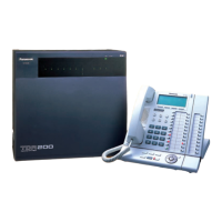
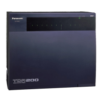
KX-TDA200BX
 Loading...