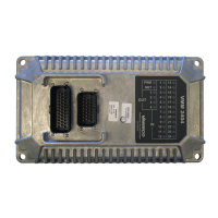
High-Side/Low-Side Output Specifications
Short circuit trip point (high-side)
Short circuit trip point (low-side)
Leakage to ground, off state
Leakage to battery, off state
Acceptable Voltage on Low Side Ground
(J2-1F with respect to J1-3A) (see note)
High-side turn on time (enable signal to 90%)
High-side turn off time (/enable signal to 10%)
High-side slew rate rising edge,
10% to 30%, Rload = 12Ω
High-side slew rate falling edge,
70% to 40%, Rload = 12Ω
Low-side turn on time (enable signal to 90%)
Low-side turn off time (/enable signal to 10%)
Low-side slew rate rising edge,
50% to 70%, Rload = 2.2Ω
Low-side slew rate falling edge,
70% to 50%, Rload = 2.2Ω
Open load detection resistance
Note: This is the voltage range over which the low side outputs will operate properly. Voltage
differences from low side ground to logic ground beyond these levels could result in the low
side outputs turning on or off unexpectedly.
The outputs have the ability to be programmed for PWM duty cycles, excluding
H-Bridge.
The outputs have a single programmable frequency which is shared with
OUTPUT1_10A_HS to OUTPUT8_10A_HS.
 Loading...