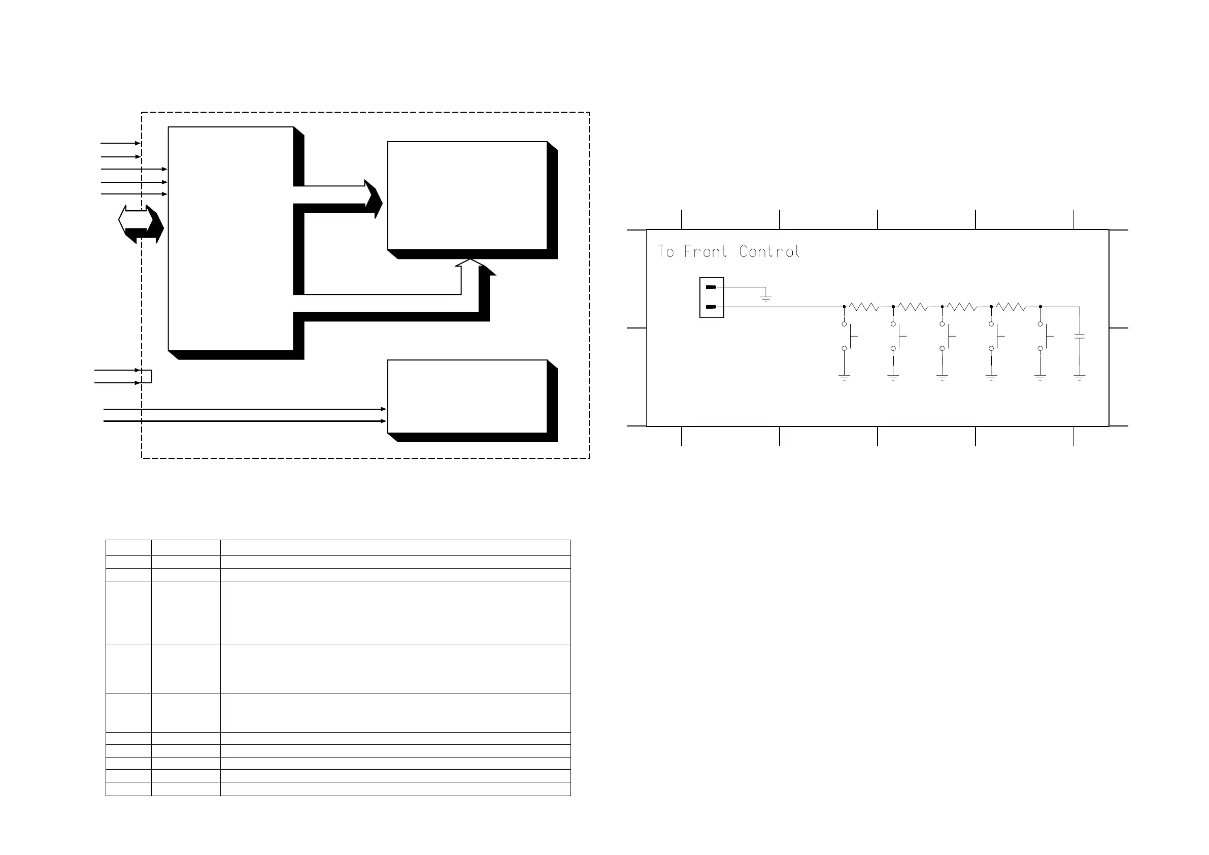
VOLUME FTD DISPLAY PIN CONFIGURATION
6-2 6-2
DTC KEY PART - CIRCUIT DIAGRAM
1234
1234
A
B
A
B
1400 A1
1401 A2
1402 B3
1403 B3
1404 A4
1405 B4
2400 B4
3400 A2
3401 A3
3402 A3
3403 A4
GND_B
2
GND_B
100p
2400
GND_B
EH-S
1400
1
GND_BGND_B
GND_B
1401
DISC1
GND_B
DISC2
3400
150R
3402
270R
1402
3401
220R
1403
DISC3
DISC4
1404
DISC5
1405
3403
390R
8239 210 9413 pt4 dd wk0323
LCD Segment Display
WHITE LED BACKLIGHT
LCD CONTROLLER/
DRIVER
’HOLTEK’
HT1621
(Die form)
1
VDD
VSS
/CS
/RD
/WR
DATA
BZ1
BZ2
LED+
LED-
BLOCK DIAGRAM
Pin No.
1
2
3
4
5
6
7
8
9
10
Symbol.
VDD
VSS
/CS
/RD
/WR
DATA
LED+
LED-
BZ1
BZ2
Description
Power supply for logic circuit (+5V)
Power supply negative, ground (0V)
Chip selection input with pull-high resistor.
When the CS is logic high, the data and command read from or written to the
HT1621 are disabled. The serial interface circuit is also reset. But if CS is
at logic low level and is input to the CS pad, the data and command
transmission between the host controller and the HT1621 are all enabled.
READ clock input with pull-high resistor.
Data in the RAM of the HT1621 are clocked out on the falling edge of the RD
signal. The clocked out data will appear on the DATA line. The host controller
can use the next rising edge to latch the clocked out data.
WRITE clock input with pull-high resistor.
Data on the DATA line are latched into the HT1621 on the rising edge of the
WR signal.
Serial data input/output with pull-high resistor
Anode of backlight
Cathode of backlight
Bezel ground (connected together)
Bezel ground (connected together)
PIN CONFIGURATION