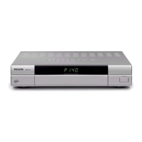
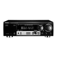
FRONT BOARDS
TABLE OF CONTENTS
FTD Display Module pin configuration ......................................................... 6-1
FTD Display Module pin configuration ......................................................... 6-2
DTC Key part - Circuit diagram .................................................................... 6-2
DTC Key part - Component & Chip layouts ................................................. 6-3
Front Display part - Circuit diagram ............................................................. 6-4
Front Display part - Component & Chip layouts .......................................... 6-5
Front Display part - Chip layout Part A ......................................................... 6-6
Front Display part - Chip layout Part B ........................................................ 6-7
Power Switch part - Circuit diagram ............................................................. 6-8
Power Switch part - Component & Chip layouts .......................................... 6-9
HDPH & Mic part - Circuit diagram ............................................................ 6-10
HDPH & Mic part - Comp. & Chip layouts.................................................. 6-11
Front Control part - Chip layout .................................................................. 6-12
Front Control part - Component layout ...................................................... 6-13
Front Control part - Circuit diagram ........................................................... 6-14
Electrical parts list....................................................................................... 6-15
6-1
6-1
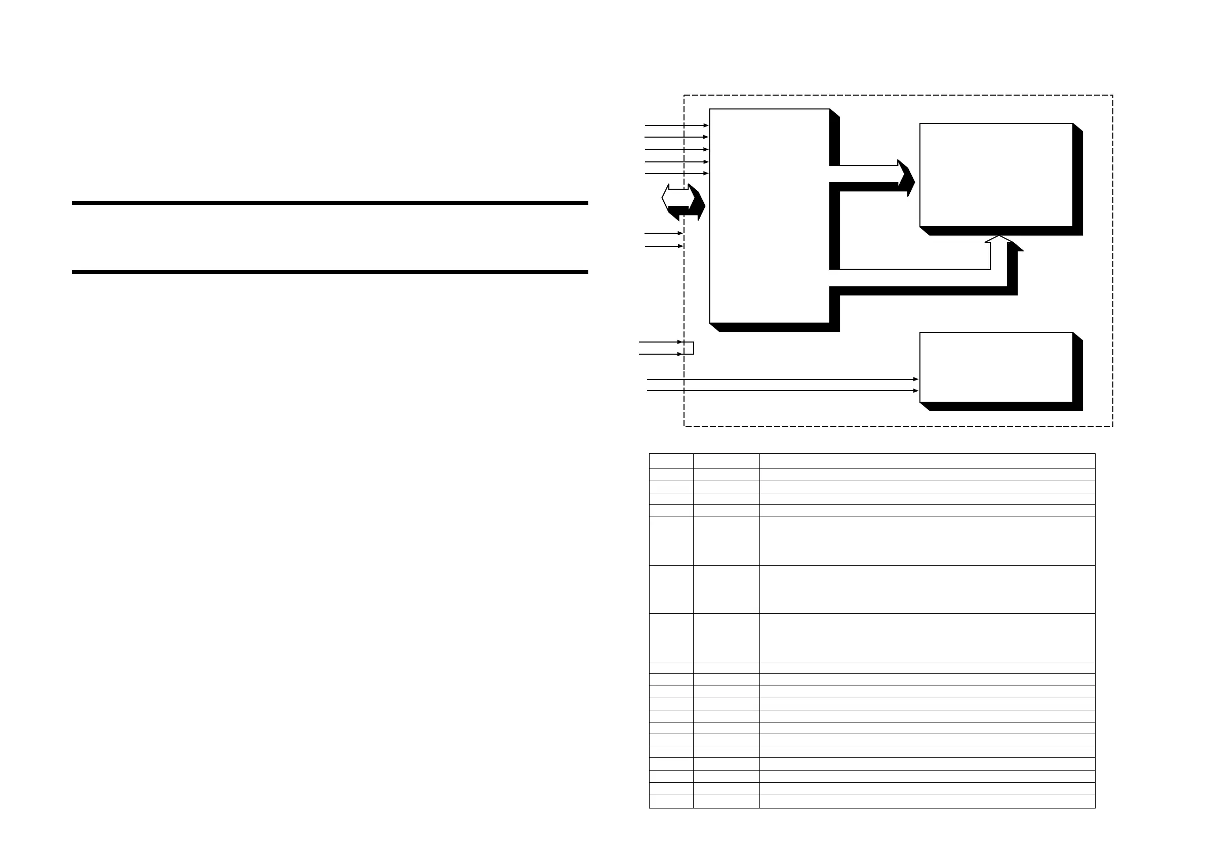
FUNCTION FTD DISPLAY PIN CONFIGURATION
LCD DISPLAY
48 X 15 DOTS + ICONS
WHITE LED BACKLIGHT
LCD CONTROLLER/
DRIVER
'SITRONIX'
ST7522
(Die form)
8
/CS1
/RES
A0
/RD
/WR
D0 - D7
VDD
VSS
BZ1
BZ2
LED+
LED-
BLOCK DIAGRAM
Pin No.
1
2
3
4
5
6
7
8
9
10
11
12
13
14
15
16
17
18
19
Symbol.
VDD
VSS
/CS1
/RES
A0
/RD
/WR
D0
D1
D2
D3
D4
D5
D6
D7
LED+
LED-
BZ1
BZ2
Description
Power supply for logic circuit (+5V)
Ground (0V)
Input, when /CS1 = 0, the chip select become active
Input low active, System reset
Usually connected to the low-order bit of the MPU address bus and used
to identify the data or a command.
A0=1: D0 - D7 are display data
A0=0: D0 - D7 are display control data
For the connection of 80-series MPU:
Input, Active low
The /RD signal of the 80-series MPU is entered in this pin. When this
signal is kept low, the ST7522 data bus is in the output status.
For the connection of 80-series MPU:
Input, Active low
The /WR signal of the 80-series MPU is entered in this pin. A signal on
the data bus is fetched at the rising edge of /WR signal.
Data input/output (LSB)
Data input/output
Data input/output
Data input/output
Data input/output
Data input/output
Data input/output
Data input/output (MSB)
Anode of backlight
Cathode of backlight
Bezel ground (connected together)
Bezel ground (connected together)
PIN CONFIGURATION