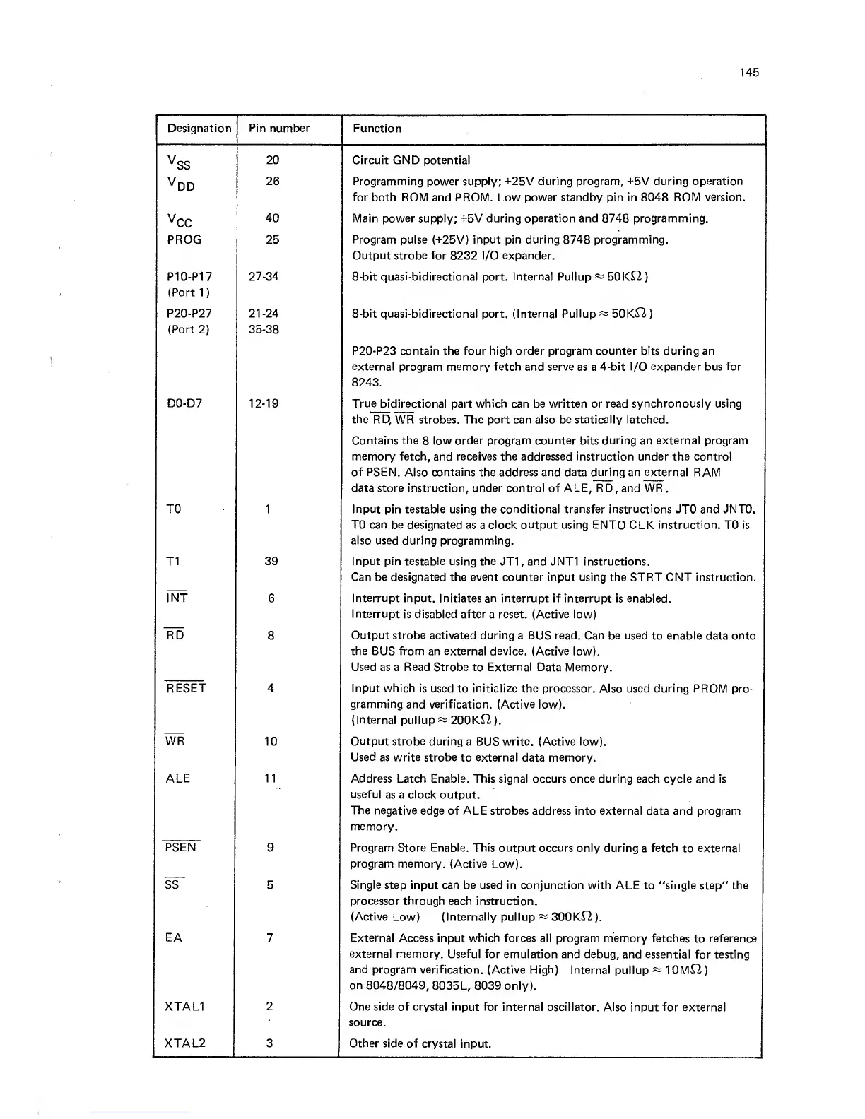
Designation Pin number Function
^SS
20 Circuit GND potential
^DD
26 Programming
power
supply;
-I-25V
during program,
+5V
during
operation
for both
ROM
and
PROM.
Low power standby pin in 8048 ROM
version.
^CC
40
Main power supply;
-t5V
during operation and
8748
programming.
PROG 25
Program
pulse
(-t25V)
input pin
during
8748
programming.
Output strobe for
8232 I/O
expander.
P10-P17
(Port
1
)
27-34
8-bit
quasi-bidirectional
port. Internal Pullup 50K^2
)
P20-P27
21-24
8-bit
quasi-bidirectional port. (Internal
Pullup
<=»
50K^2
)
(Port
2)
35-38
P20-P23 contain
the four
high order program counter bits
during
an
external program memory fetch and serve
as a
4-bit I/O
expander
bus
for
8243.
D0-D7
12-19
True
bidirectional part
which
can be written or read
synchronously
using
the
RD,
WR
strobes. The port can also be statically latched.
Contains the
8
low order program counter bits during an external program
memory fetch,
and
receives the addressed instruction under
the
control
of PSEN.
Also contains the address and data during an external RAM
data store instruction, under
control
of
ALE, RD, and WR.
TO
1
Input pin
testable using
the
conditional transfer instructions JTO and
JNTO.
TO can be designated
as a
clock output using
ENTO CLK instruction. TO is
also used during programming.
T1 39 Input pin testable using the
JT1,
and
JNT1
instructions.
Can
be
designated
the
event
counter input using the STRT
CNT
instruction.
6
Interrupt
input. Initiates an interrupt if interrupt is enabled.
Interrupt
is
disabled after
a reset. (Active low)
8
Output
strobe
activated during a BUS read. Can be used
to
enable
data onto
the BUS from an external device. (Active
low).
Used
as a Read Strobe to External Data Memory.
RESET 4 Input which is
used to
initialize
the processor. Also used during
PROM pro-
gramming and verification. (Active
low).
(Internal
pullup 200KJ2
).
WR 10 Output strobe
during a BUS write. (Active low).
Used as write strobe
to
external
data
memory.
ALE 11 Address
Latch Enable. This signal occurs once
during each cycle and is
useful
as a clock output.
The negative
edge of ALE strobes address into external
data and program
memory.
PSEN
9 Program Store Enable. This output
occurs only during
a
fetch
to
external
program
memory. (Active Low).
5
Single step input
can be used in conjunction with
ALE to "single step" the
processor through
each instruction.
(Active
Low)
(internally
pullup 300K^2
).
EA
7 External Access input which
forces all program memory
fetches
to
reference
external
memory. Useful for
emulation and debug,
and
essential
for testing
and program verification.
(Active High) Internal
pullup
^
10MJ2)
on
8048/8049, 8035
L,
8039 only).
XTAL1
2
One side of crystal input for
internal oscillator. Also input for
external
source.
XTAL2 3 Other side of crystal
input.