56
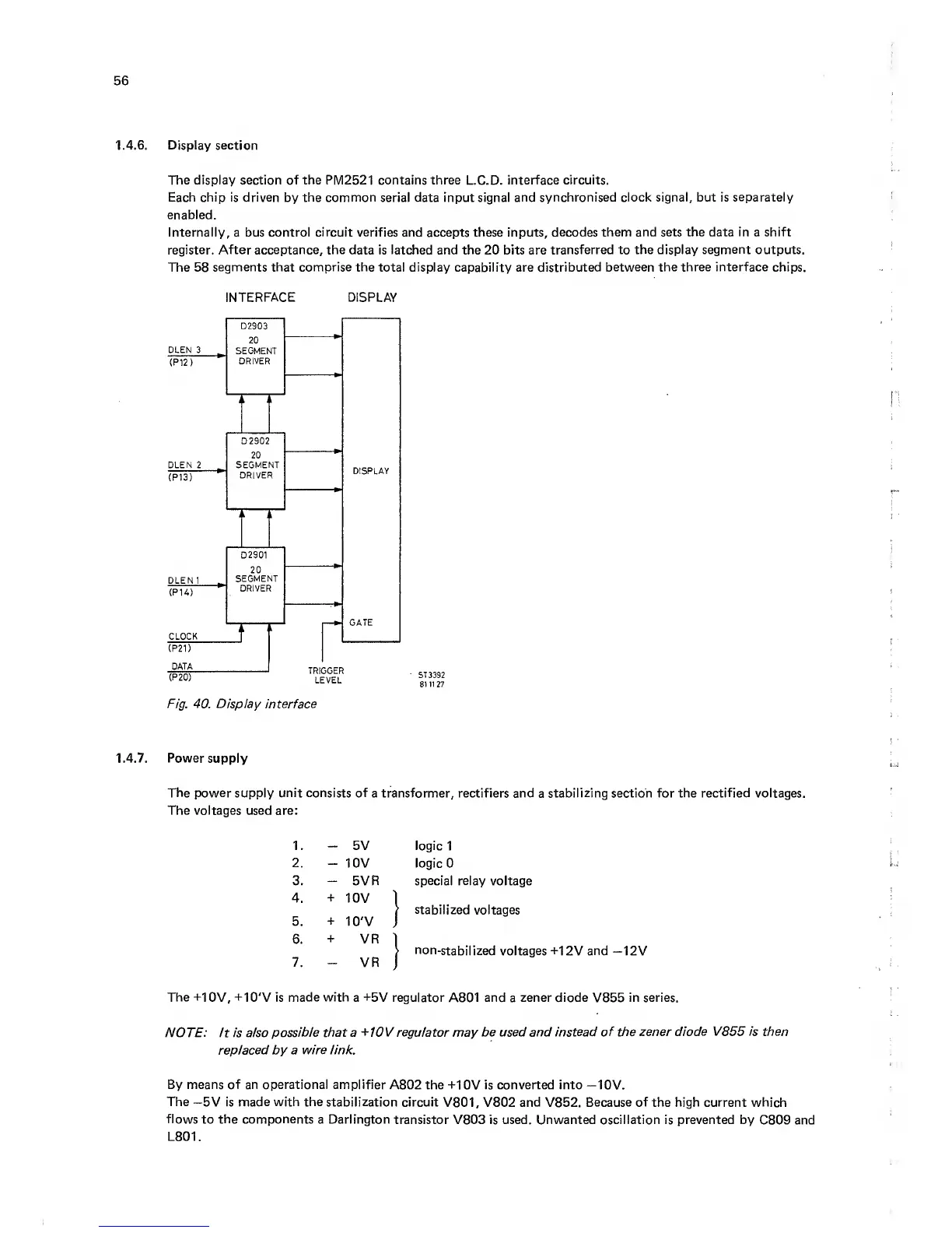
1.4.6. Display section
The display section of the PM2521 contains three
L.C.D.
interface circuits.
Each chip is driven
by
the common
serial data input signal
and synchronised clock signal, but is
separately
enabled.
Internally, a bus control
circuit verifies
and accepts these inputs,
decodes them and sets the data in a shift
register. After acceptance, the
data is
latched
and the 20 bits are
transferred to the display
segment
outputs.
The 58
segments that comprise the
total display capability are distributed
between the three interface
chips.
INTERFACE DISPLAY
Fig. 40. Display
interface
1.4.7. Power
supply
The power supply unit consists of
a transformer, rectifiers and
a
stabilizing
section for the
rectified
voltages.
The voltages used are:
1.
-
5V logic
1
2.
-
10V logic 0
3.
-
5VR
special relay
voltage
4.
+
10V
1
I
stabilized voltages
5.
+
10'V
J
6.
+
VR
1
t
1
non-stabilized
voltages
+12V
and
7.
—
VR
j
The
+10V, +10'V is
made with
a +5V regulator
A801
and
a
zener diode
V855
in series.
NOTE: It is also
possible that a
+10V regulator
may
be used and instead
of the zener diode
V855 is
then
replaced
by
a wire link.
By means of an operational amplifier
A802 the
+10V
is converted into
—10V.
The
—
5V is
made with the stabilization
circuit
V801, V802
and
V852.
Because of
the high
current
which
flows
to
the components
a Darlington
transistor V803 is used. Unwanted oscillation is prevented by
C809 and
L801.